| HPC connector pin summary | |
| General pin function | Pin count |
| Gigabit data | 40 |
| Gigabit clocks | 4 |
| User data | 160 |
| User clocks | 8 |
| I2C | 2 |
| JTAG | 5 |
| State flags | 5 |
| Power supply | 15 |
| Ground | 159 |
| Reserved | 2 |
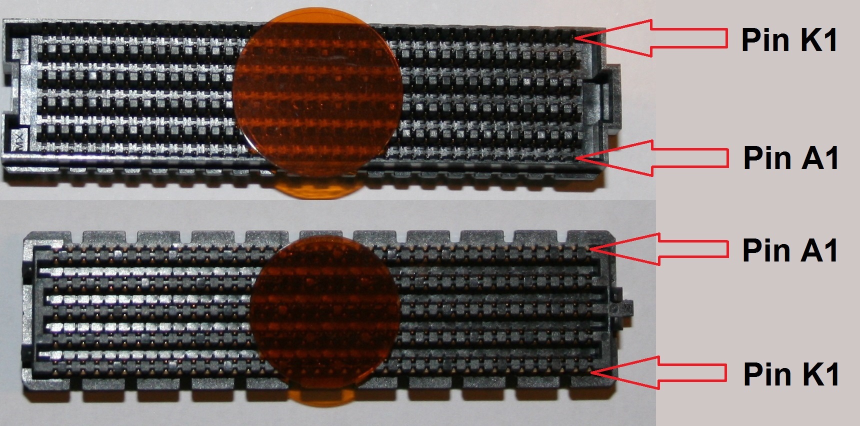
 Footprints can be viewed in Lib_Altium repository.
| K | J | H | G | F | E | D | C | B | A | |
| 1 | VREF_B_M2C | GND | VREF_A_M2C | GND | PG_M2C | GND | PG_C2M | GND | CLK_DIR | GND |
| 2 | GND | CLK3_BIDIR_P | PRSNT_M2C_L | CLK1_M2C_P | GND | HA01_P_CC | GND | DP0_C2M_P | GND | DP1_M2C_P |
| 3 | GND | CLK3_BIDIR_N | GND | CLK1_M2C_N | GND | HA01_N_CC | GND | DP0_C2M_N | GND | DP1_M2C_N |
| 4 | CLK2_BIDIR_P | GND | CLK0_M2C_P | GND | HA00_P_CC | GND | GBTCLK0_M2C_P | GND | DP9_M2C_P | GND |
| 5 | CLK2_BIDIR_N | GND | CLK0_M2C_N | GND | HA00_N_CC | GND | GBTCLK0_M2C_N | GND | DP9_M2C_N | GND |
| 6 | GND | HA03_P | GND | LA00_P_CC | GND | HA05_P | GND | DP0_M2C_P | GND | DP2_M2C_P |
| 7 | HA02_P | HA03_N | LA02_P | LA00_N_CC | HA04_P | HA05_N | GND | DP0_M2C_N | GND | DP2_M2C_N |
| 8 | HA02_N | GND | LA02_N | GND | HA04_N | GND | LA01_P_CC | GND | DP8_M2C_P | GND |
| 9 | GND | HA07_P | GND | LA03_P | GND | HA09_P | LA01_N_CC | GND | DP8_M2C_N | GND |
| 10 | HA06_P | HA07_N | LA04_P | LA03_N | HA08_P | HA09_N | GND | LA06_P | GND | DP3_M2C_P |
| 11 | HA06_N | GND | LA04_N | GND | HA08_N | GND | LA05_P | LA06_N | GND | DP3_M2C_N |
| 12 | GND | HA11_P | GND | LA08_P | GND | HA13_P | LA05_N | GND | DP7_M2C_P | GND |
| 13 | HA10_P | HA11_N | LA07_P | LA08_N | HA12_P | HA13_N | GND | GND | DP7_M2C_N | GND |
| 14 | HA10_N | GND | LA07_N | GND | HA12_N | GND | LA09_P | LA10_P | GND | DP4_M2C_P |
| 15 | GND | HA14_P | GND | LA12_P | GND | HA16_P | LA09_N | LA10_N | GND | DP4_M2C_N |
| 16 | HA17_P_CC | HA14_N | LA11_P | LA12_N | HA15_P | HA16_N | GND | GND | DP6_M2C_P | GND |
| 17 | HA17_N_CC | GND | LA11_N | GND | HA15_N | GND | LA13_P | GND | DP6_M2C_N | GND |
| 18 | GND | HA18_P | GND | LA16_P | GND | HA20_P | LA13_N | LA14_P | GND | DP5_M2C_P |
| 19 | HA21_P | HA18_N | LA15_P | LA16_N | HA19_P | HA20_N | GND | LA14_N | GND | DP5_M2C_N |
| 20 | HA21_N | GND | LA15_N | GND | HA19_N | GND | LA17_P_CC | GND | GBTCLK1_M2C_P | GND |
| 21 | GND | HA22_P | GND | LA20_P | GND | HB03_P | LA17_N_CC | GND | GBTCLK1_M2C_N | GND |
| 22 | HA23_P | HA22_N | LA19_P | LA20_N | HB02_P | HB03_N | GND | LA18_P_CC | GND | DP1_C2M_P |
| 23 | HA23_N | GND | LA19_N | GND | HB02_N | GND | LA23_P | LA18_N_CC | GND | DP1_C2M_N |
| 24 | GND | HB01_P | GND | LA22_P | GND | HB05_P | LA23_N | GND | DP9_C2M_P | GND |
| 25 | HB00_P_CC | HB01_N | LA21_P | LA22_N | HB04_P | HB05_N | GND | GND | DP9_C2M_N | GND |
| 26 | HB00_N_CC | GND | LA21_N | GND | HB04_N | GND | LA26_P | LA27_P | GND | DP2_C2M_P |
| 27 | GND | HB07_P | GND | LA25_P | GND | HB09_P | LA26_N | LA27_N | GND | DP2_C2M_N |
| 28 | HB06_P_CC | HB07_N | LA24_P | LA25_N | HB08_P | HB09_N | GND | GND | DP8_C2M_P | GND |
| 29 | HB06_N_CC | GND | LA24_N | GND | HB08_N | GND | TCK | GND | DP8_C2M_N | GND |
| 30 | GND | HB11_P | GND | LA29_P | GND | HB13_P | TDI | SCL | GND | DP3_C2M_P |
| 31 | HB10_P | HB11_N | LA28_P | LA29_N | HB12_P | HB13_N | TDO | SDA | GND | DP3_C2M_N |
| 32 | HB10_N | GND | LA28_N | GND | HB12_N | GND | 3P3VAUX | GND | DP7_C2M_P | GND |
| 33 | GND | HB15_P | GND | LA31_P | GND | HB19_P | TMS | GND | DP7_C2M_N | GND |
| 34 | HB14_P | HB15_N | LA30_P | LA31_N | HB16_P | HB19_N | TRST_L | GA0 | GND | DP4_C2M_P |
| 35 | HB14_N | GND | LA30_N | GND | HB16_N | GND | GA1 | 12P0V | GND | DP4_C2M_N |
| 36 | GND | HB18_P | GND | LA33_P | GND | HB21_P | 3P3V | GND | DP6_C2M_P | GND |
| 37 | HB17_P_CC | HB18_N | LA32_P | LA33_N | HB20_P | HB21_N | GND | 12P0V | DP6_C2M_N | GND |
| 38 | HB17_N_CC | GND | LA32_N | GND | HB20_N | GND | 3P3V | GND | GND | DP5_C2M_P |
| 39 | GND | VIO_B_M2C | GND | VADJ | GND | VADJ | GND | 3P3V | GND | DP5_C2M_N |
| 40 | VIO_B_M2C | GND | VADJ | GND | VADJ | GND | 3P3V | GND | RES0 | GND |
| LPC connector pin summary | |
| General pin function | Pin count |
| Gigabit data | 4 |
| Gigabit clocks | 2 |
| User data | 68 |
| User clocks | 4 |
| I2C | 2 |
| JTAG | 5 |
| State flags | 4 |
| Power supply | 10 |
| Ground | 61 |
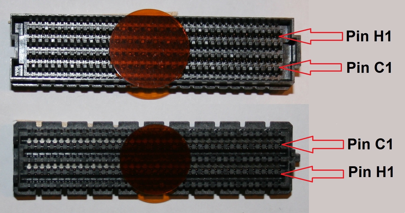
 Footprints can be viewed in Lib_Altium repository.
| K | J | H | G | F | E | D | C | B | A | |
| 1 | VREF_A_M2C | GND | PG_C2M | GND | ||||||
| 2 | PRSNT_M2C_L | CLK1_M2C_P | GND | DP0_C2M_P | ||||||
| 3 | GND | CLK1_M2C_N | GND | DP0_C2M_N | ||||||
| 4 | CLK0_M2C_P | GND | GBTCLK0_M2C_P | GND | ||||||
| 5 | CLK0_M2C_N | GND | GBTCLK0_M2C_N | GND | ||||||
| 6 | GND | LA00_P_CC | GND | DP0_M2C_P | ||||||
| 7 | LA02_P | LA00_N_CC | GND | DP0_M2C_N | ||||||
| 8 | LA02_N | GND | LA01_P_CC | GND | ||||||
| 9 | GND | LA03_P | LA01_N_CC | GND | ||||||
| 10 | LA04_P | LA03_N | GND | LA06_P | ||||||
| 11 | LA04_N | GND | LA05_P | LA06_N | ||||||
| 12 | GND | LA08_P | LA05_N | GND | ||||||
| 13 | LA07_P | LA08_N | GND | GND | ||||||
| 14 | LA07_N | GND | LA09_P | LA10_P | ||||||
| 15 | GND | LA12_P | LA09_N | LA10_N | ||||||
| 16 | LA11_P | LA12_N | GND | GND | ||||||
| 17 | LA11_N | GND | LA13_P | GND | ||||||
| 18 | GND | LA16_P | LA13_N | LA14_P | ||||||
| 19 | LA15_P | LA16_N | GND | LA14_N | ||||||
| 20 | LA15_N | GND | LA17_P_CC | GND | ||||||
| 21 | GND | LA20_P | LA17_N_CC | GND | ||||||
| 22 | LA19_P | LA20_N | GND | LA18_P_CC | ||||||
| 23 | LA19_N | GND | LA23_P | LA18_N_CC | ||||||
| 24 | GND | LA22_P | LA23_N | GND | ||||||
| 25 | LA21_P | LA22_N | GND | GND | ||||||
| 26 | LA21_N | GND | LA26_P | LA27_P | ||||||
| 27 | GND | LA25_P | LA26_N | LA27_N | ||||||
| 28 | LA24_P | LA25_N | GND | GND | ||||||
| 29 | LA24_N | GND | TCK | GND | ||||||
| 30 | GND | LA29_P | TDI | SCL | ||||||
| 31 | LA28_P | LA29_N | TDO | SDA | ||||||
| 32 | LA28_N | GND | 3P3VAUX | GND | ||||||
| 33 | GND | LA31_P | TMS | GND | ||||||
| 34 | LA30_P | LA31_N | TRST_L | GA0 | ||||||
| 35 | LA30_N | GND | GA1 | 12P0V | ||||||
| 36 | GND | LA33_P | 3P3V | GND | ||||||
| 37 | LA32_P | LA33_N | GND | 12P0V | ||||||
| 38 | LA32_N | GND | 3P3V | GND | ||||||
| 39 | GND | VADJ | GND | 3P3V | ||||||
| 40 | VADJ | GND | 3P3V | GND |
| LA[00..33]_P, LA[00..33]_N |
LA_XX - LPC, FPGA Bank A,68 user-defined, single-ended signals or 34 user-defined, differential pairs (mandatory for LPC) |
| HA[00..23]_P, HA[00..23]_N |
HA_XX - HPC, FPGA Bank A,48 user-defined, single-ended signals or 24 user-defined, differential pairs |
| HB[00..21]_P, HB[00..21]_N |
HB_XX - HPC, FPGA Bank B,44 user-defined, single-ended signals or 22 user-defined, differential pairs |
| XX_P_CC, XX_N_CC |
User-defined clock capable (CC) pins. These pins can be used for clock signals. |
| CLK[0..1]_M2C_P, CLK[0..1]_M2C_N |
2 user clocks, differential pairs, driver is the mezzanine module |
| CLK[2..3]_BIDIR_P, CLK[2..3]_BIDIR_N |
2 user clocks, differential pairs, bidirectional (driver is determined by CLK_DIR pin) |
| CLK_DIR | Determines the driver for CLK[2..3]_BIDIR. GND (or floating) if the mezzanine module is the driver. 3P3V via 10k pull-up resistor if the carrier card drives the clock signals. Connection is made on the mezzanine module. |
| GBTCLK[0..1]_M2C_P, GBTCLK[0..1]_M2C_N |
Clock signals for multi-gigabit transceiver data pairs (GBTCLK1_x only for HPC) |
| DP[0..9]_M2C_P, DP[0..9]_M2C_N |
multi-gigabit transceiver data pairs (one is mandatory for LPC, 10 in total with HPC) |
| DP[0..9]_C2M_P, DP[0..9]_C2M_N |
multi-gigabit transceiver data pairs (one is mandatory for LPC, 10 in total with HPC) |
| GA[0..1] | Geographical address of the module (can be used for adressing on I2C bus). These pins are driven by the carrier card. |
| VREF_A_M2C | Reference voltage for signaling standard of bank A (LAxx and HAxx). Can be left floating, if not required. |
| VREF_B_M2C | Reference voltage for signaling standard of bank B (HBxx). Can be left floating, if not required. |
| VIO_B_M2C | This voltage is sourced by the mezzanine module which supports the HB bus. It is used to power the IO Bank of the FPGA. |
| 3P3VAUX | 3.3 V auxiliary power supply (max. 20 mA, max. 150 uF cap. load). |
| VADJ | Adjustable voltage level (0 .. 3.3 V) from the carrier to the mezzanine card (max. 4 A, max. 1000 uF cap. load). |
| 3P3V | 3.3 V power from the carrier to the mezzanine card (max. 3 A, max. 1000 uF cap. load). |
| 12P0V | 12 V power from the carrier to the mezzanine card (max. 1 A, max. 1000 uF cap. load). |
| TRST_L | JTAG Reset |
| TCK | JTAG Clock |
| TMS | JTAG Mode Select |
| TDI | JTAG Data In, if JTAG chain is not used by mezzanine card, short TDI and TDO. |
| TDO | JTAG Data Out, if JTAG chain is not used by mezzanine card, short TDI and TDO. |
| PRSNT_M2C_L | Present signal. Indicates that a mezzanine module is attached to the carrier. Low active (tie to GND on FMC) |
| PG_C2M | Active high power good signal. High indicates that VADJ, 12P0V, and 3P3V are within tolerance. |
| PG_M2C | Active high power good signal. High indicates that VIO_B_M2C, VREF_A_M2C, and VREF_B_M2C are within tolerance. |
| SCL | I2C serial clock. Interface can support Intelligent Platform Management Interface (IPMI) commands. |
| SDA | I2C serial data. Interface can support Intelligent Platform Management Interface (IPMI) commands. |
| RES[0..1] | Reserved, left floating |
| GND | Signal ground |
| _M2C_ | Mezzanine-to-Carrier, signal is driven by the mezzanine module and received by the carrier card |
| _C2M_ | Carrier-to-Mezzanine, signal is driven by the carrier card and received by the mezzanine module |
| 1 | ANSI/VITA 57.1-2008 |
| 2 | Overview of VITA57 – FMC, Curtiss Wright, www.vita.com/Resources/Learn/FMC%20Overview.pptx |
| 3 | KC705 Evaluation Board for the Kintex-7 FPGA, Xilinx UG810 |
| 4 | I/O Design Flexibility with the FPGA Mezzanine Card (FMC), Xilinx WP315 |
| 5 | FMC LPC and HPC connector Excel sheet |
| 6 | FMCHUB - FPGA MEZZANINE CARDs |
| 7 | Lib_Altium, Altium Designer libraries for ANSI/VITA 57 FPGA Mezzanine Card (FMC) Standard |
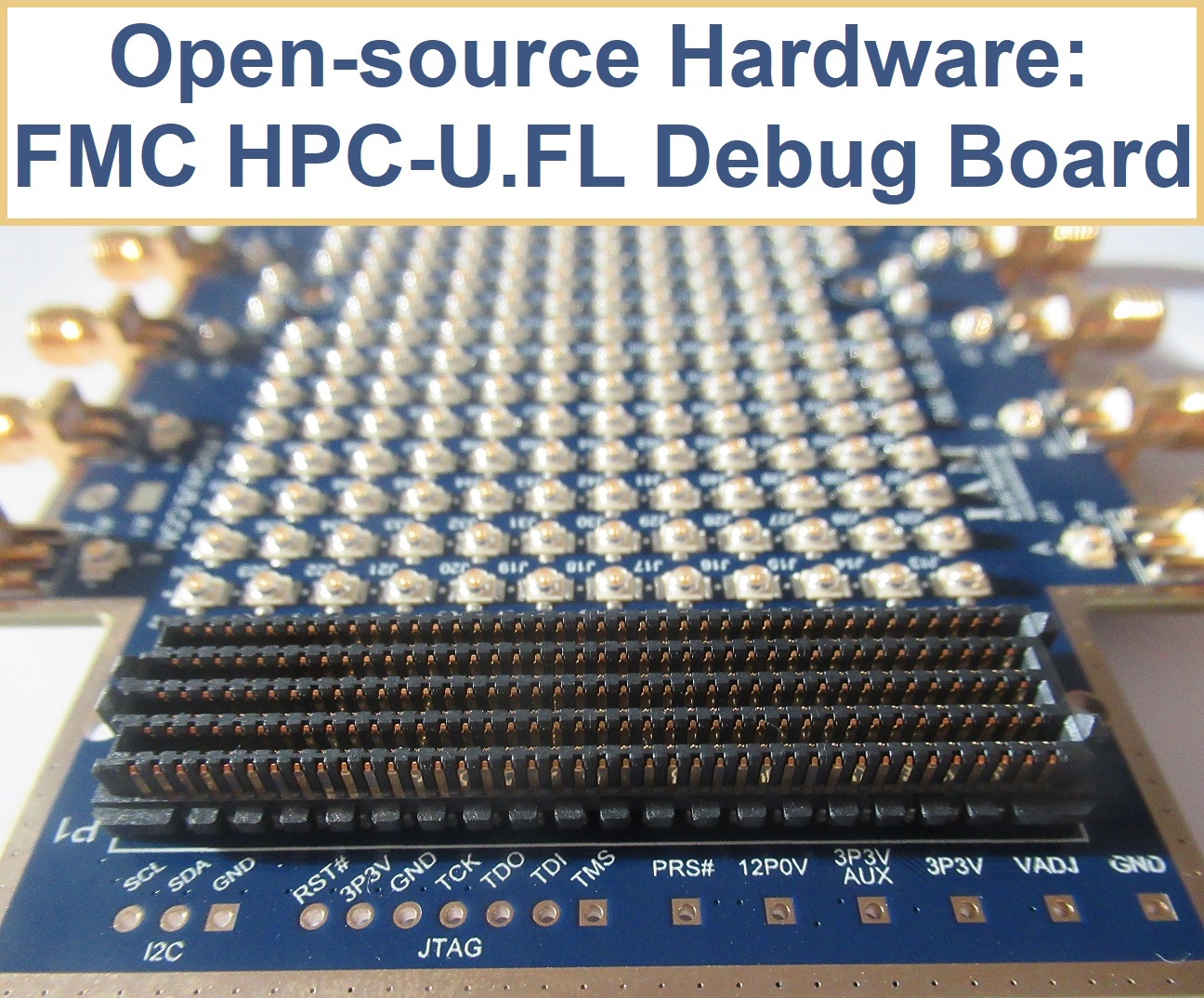
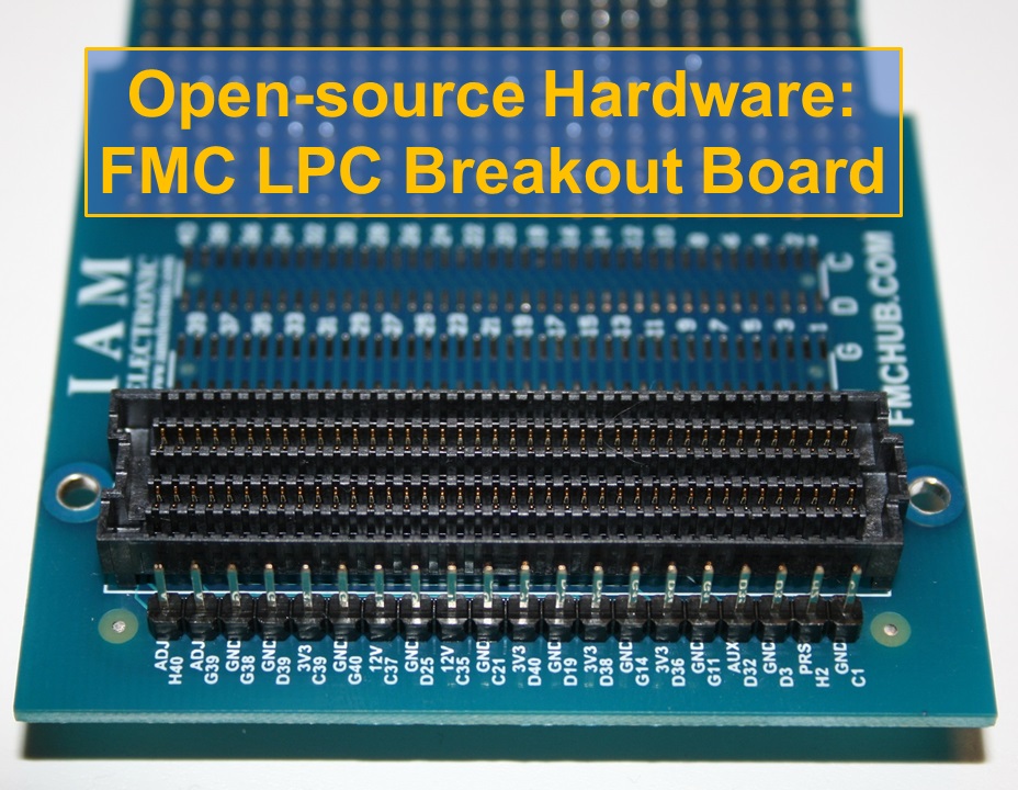
| 8 | FMC LPC Breakout board, Datasheet of Open-source hardware FMC module |
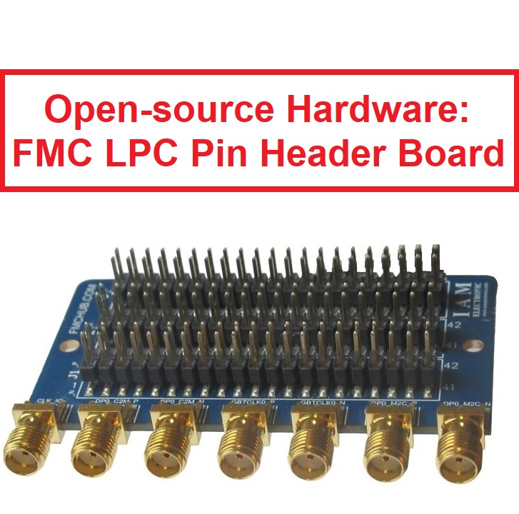
| 9 | FMC LPC Pin Header board, Datasheet of Open-source hardware FMC module |
| 10 | FMC HPC to LPC Breakout board, Datasheet of Open-source hardware FMC module |