- ANSI/VITA 57.1 compliant
- Commercial grade form factor
- Low-pin count (LPC) connectors
- Breakout of carrier card connector
- Breakout of mezzanine card connector
- Stackable assembly
- Separate breakout of power pins
- Breakout pads with 1.27 mm pitch
- Prototyping area with 2.54 mm grid
- Open-source hardware
The photos below show the bottom side with LPC mezzanine card connector (MC-LPC-10) and top side with LPC carrier card connector (CC-LPC-10).
- Easy prototyping
- Testing and debugging of FMC modules
- Research and education with FPGAs
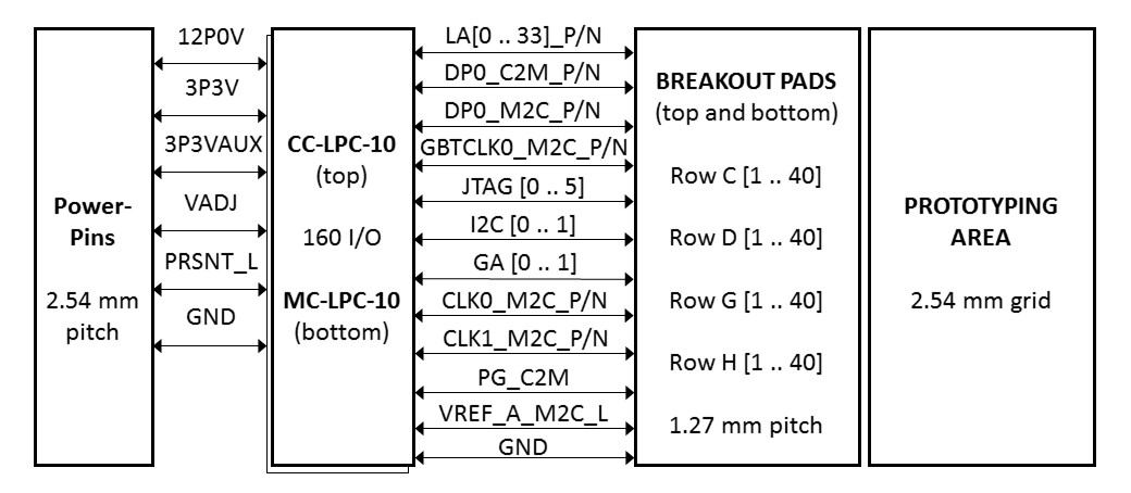
The FMC LPC Breakout board is a passive adapter for accessing all signals of ANSI/VITA 57.1 FPGA Mezzanine Card (FMC) Standard compliant low-pin count (LPC) connectors. All pins of the connector's rows C, D, G, and H are routed to a separate pad array on the top and bottom side. These pads were placed at a 1.27 mm pitch to easily attach additional probes or solder wires. For special measuring tasks or for use as a stand-alone carrier, the power pins of the connector were routed to additional vias in the back of the module. Furthermore, simple electrical circuits can be realized on the prototyping area, which is a field of non connected vias with a pitch of 2.54 mm. The FPGA mezzanine card has commercial grade form factor (single width, 78.80 mm x 69 mm) and is designed for air cooling.
The FMC LPC Breakout module is predestined for three typical applications:
1. Passive FMC module
The board can be used as a passive FMC module or breadboard. Functionality must be realised by external circuitry on the prototyping area.
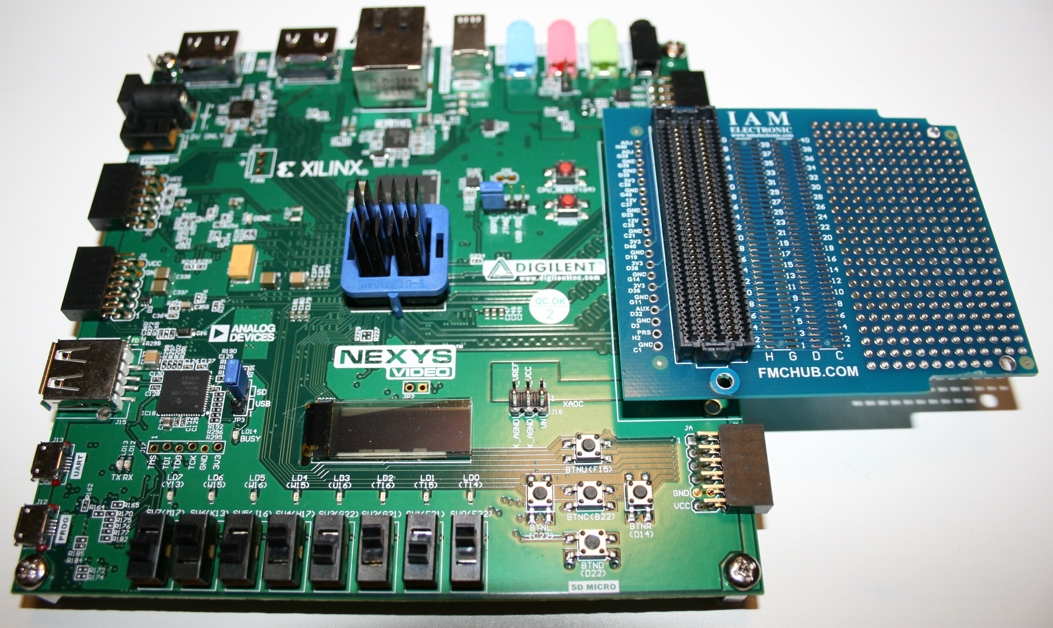 Fig. 1: FMC LPC Breakout module plugged on carrier board (Digilent Nexys Video™ Board, 410-316).
2. Simple FMC carrier The module can also be used as simple FMC carrier board. This card cannot be used to implement a whole application, but basic functions can be provided. For example, the correct behavior of an attached FMC module can be verified by providing an external power supply through the FMC LPC Breakout board. Or even a simple I2C programmer and reader for a FRU (field replaceable unit) record can be implemented with this carrier board as a basis.
3. Test point insertion (stacked assembly) The most reasonable application of the module is probably its use as an external test point array for devices under test. The connectors on the top and bottom allow the stacking of at least two external FMC boards. Thus the FMC LPC Breakout module in the middle of the stack between a carrier and mezzanine card provides test points for all signals passing through the connectors. With such a configuration, a real world FMC setup can be evaluated and debugged.
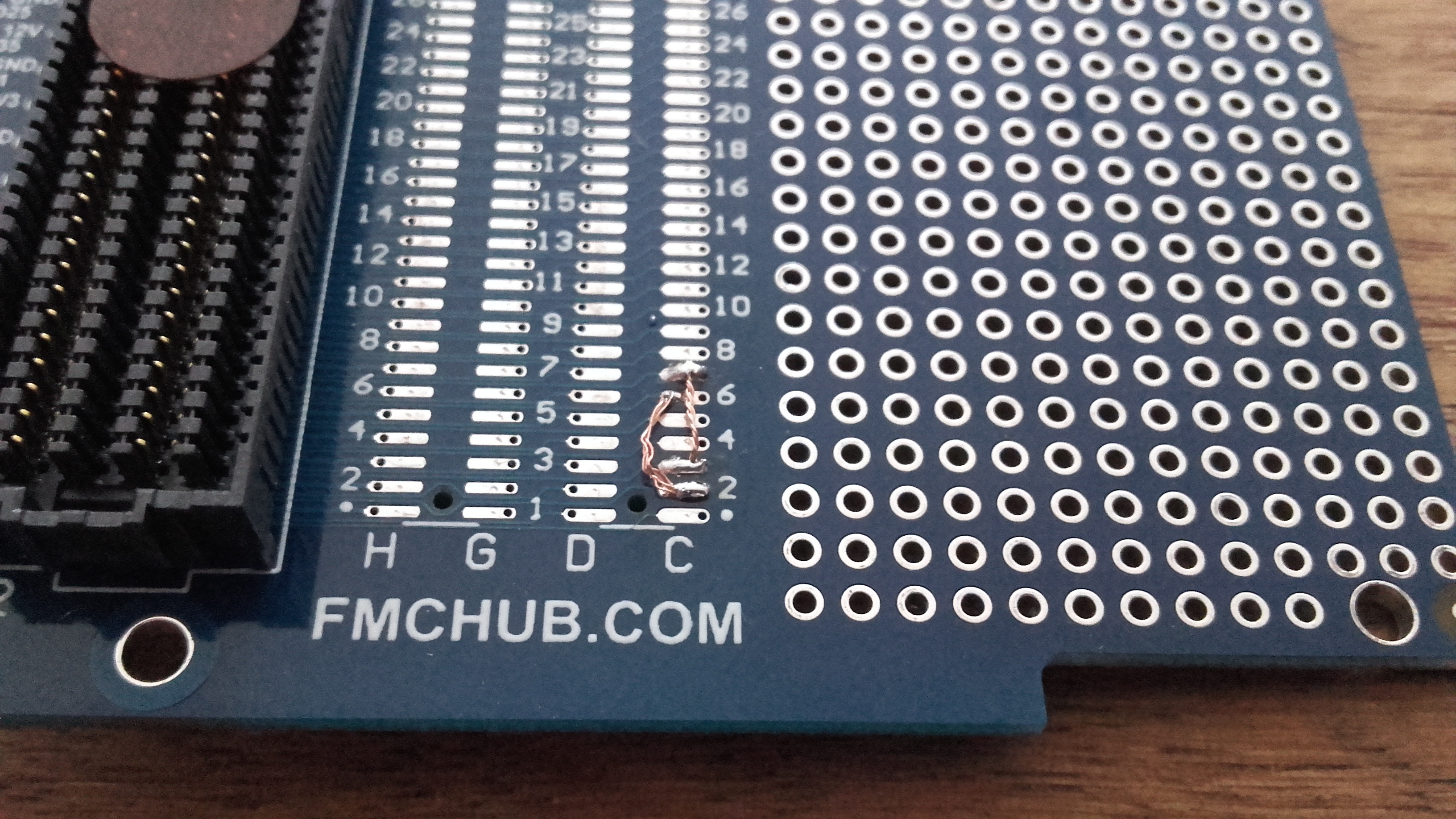
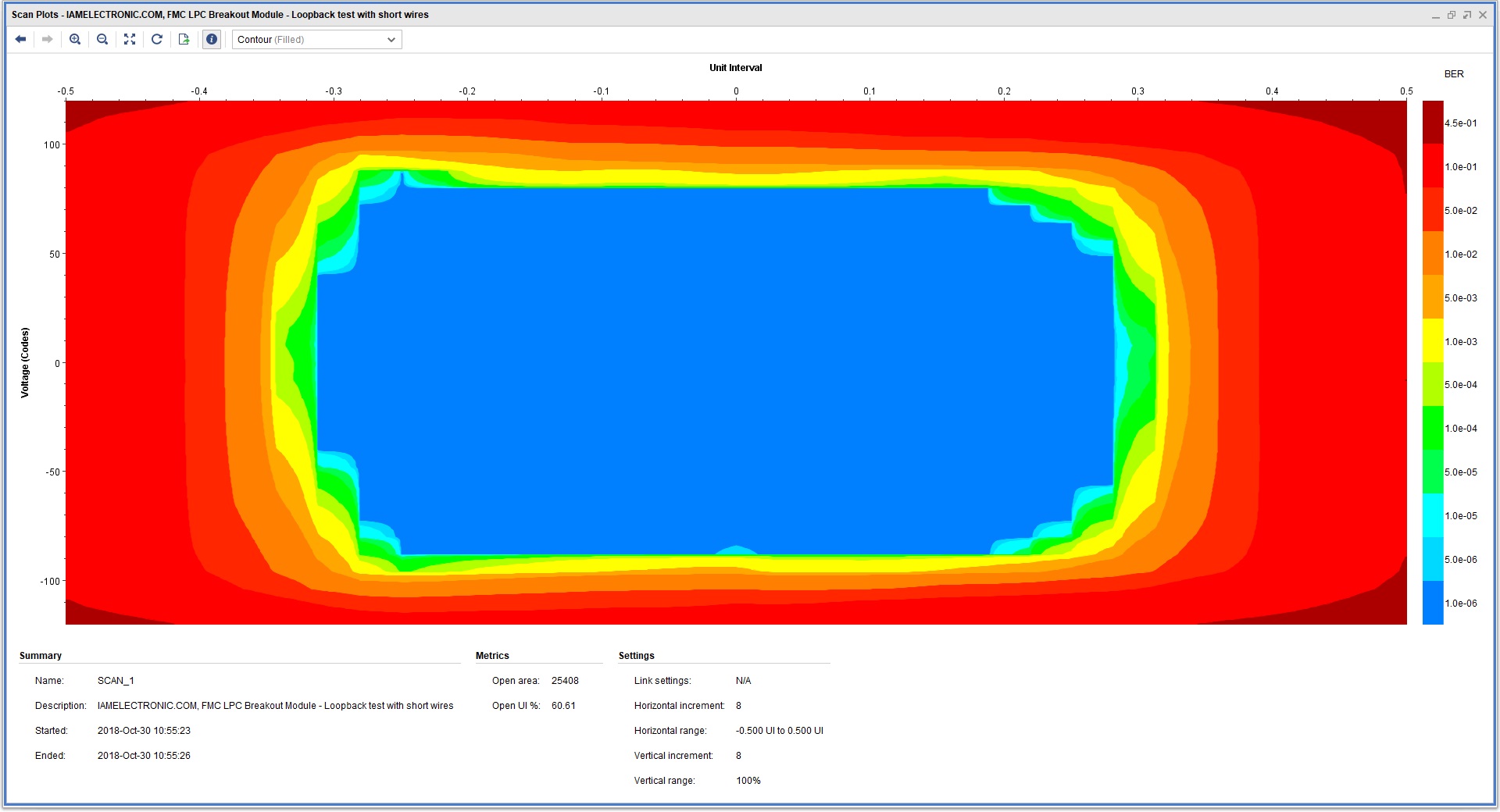
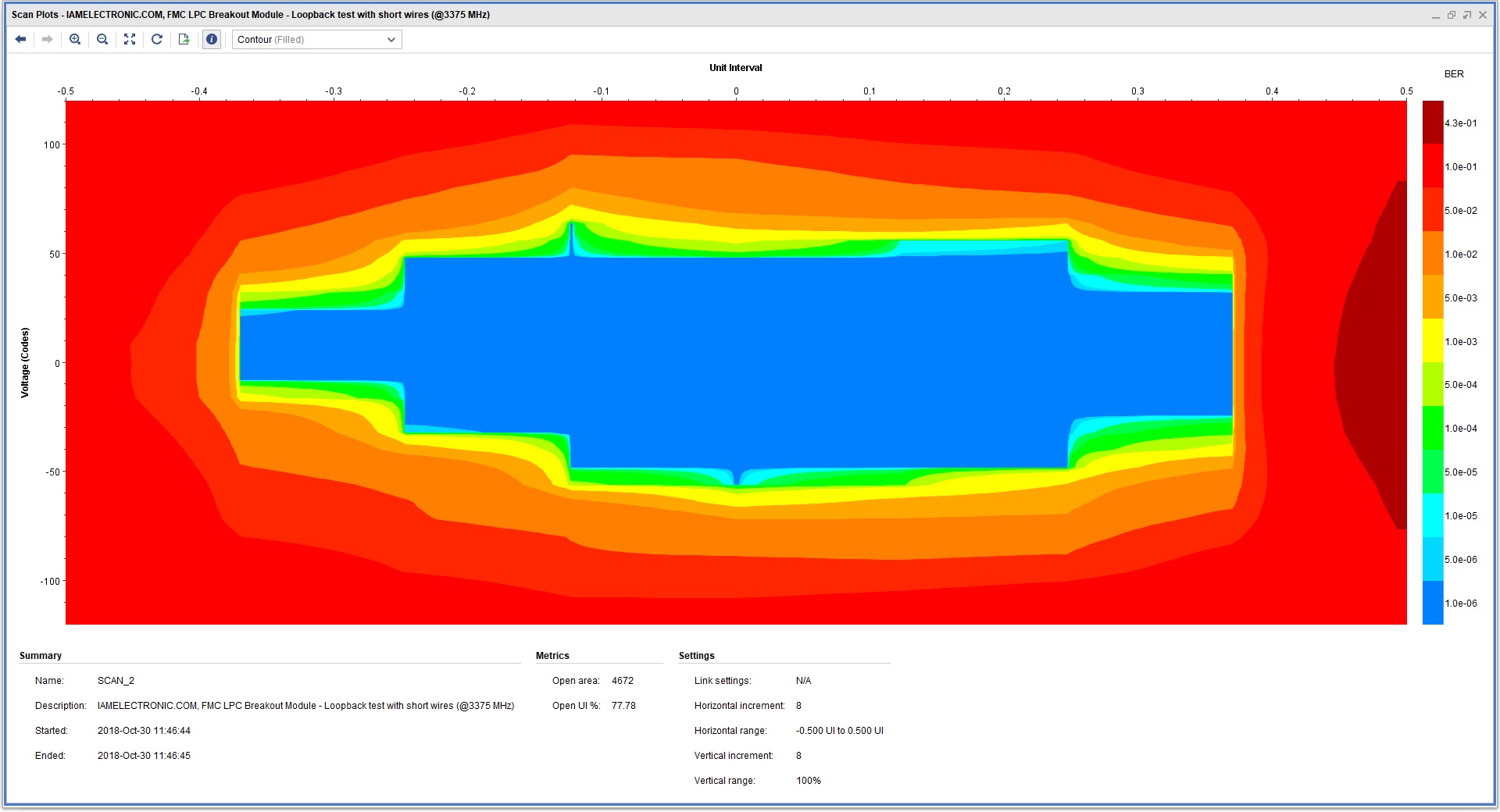
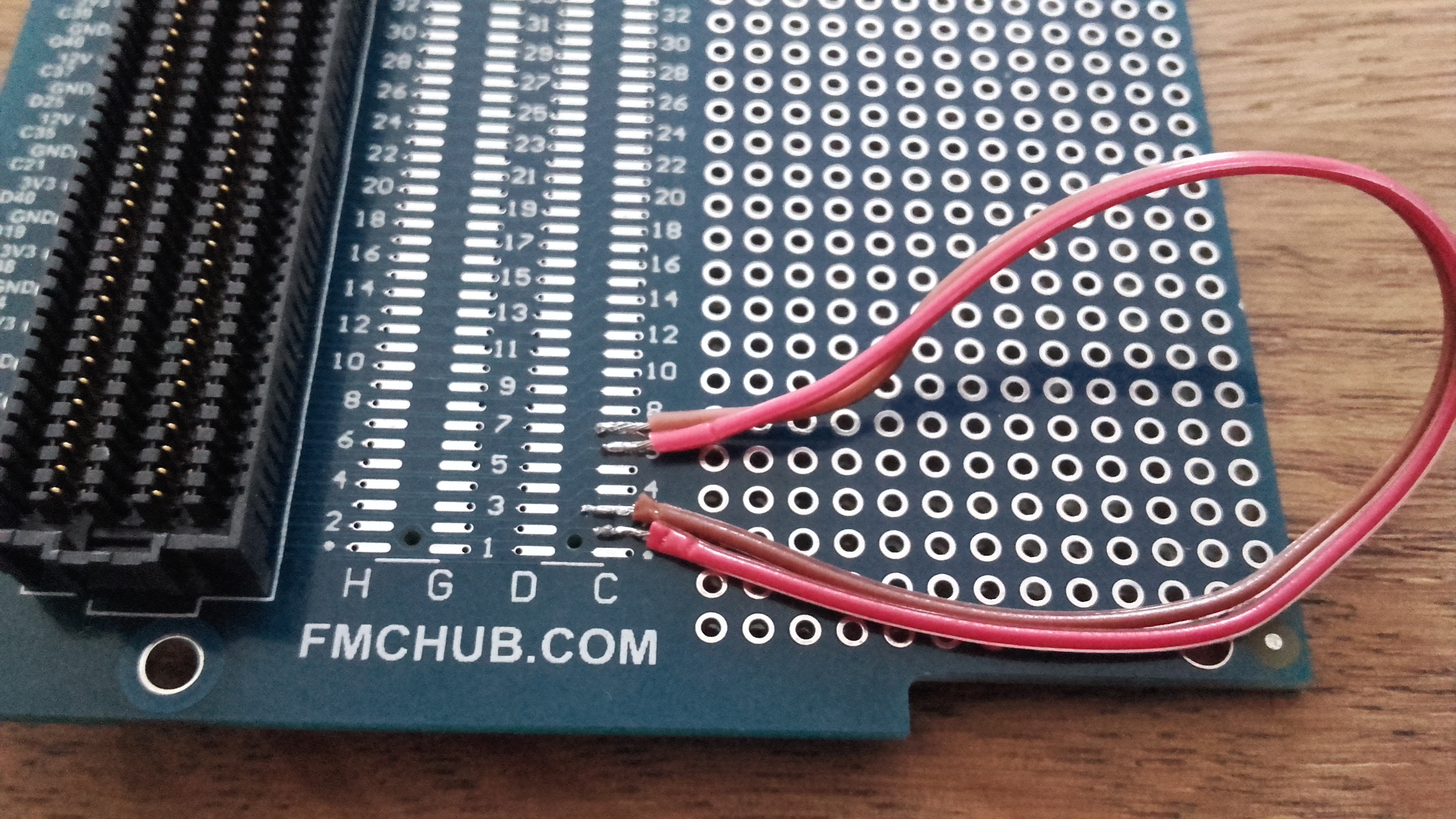
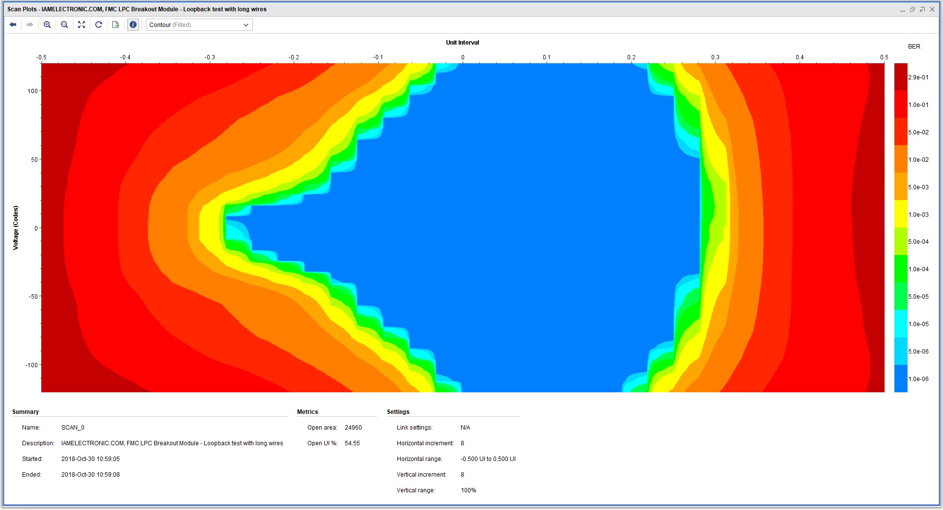
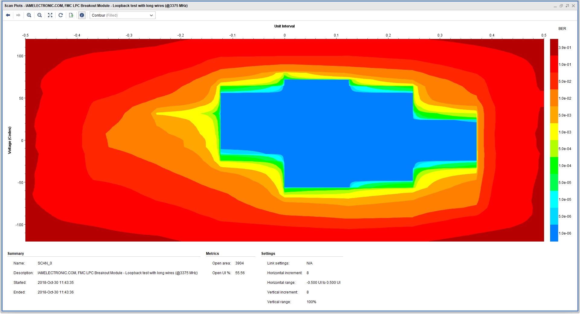
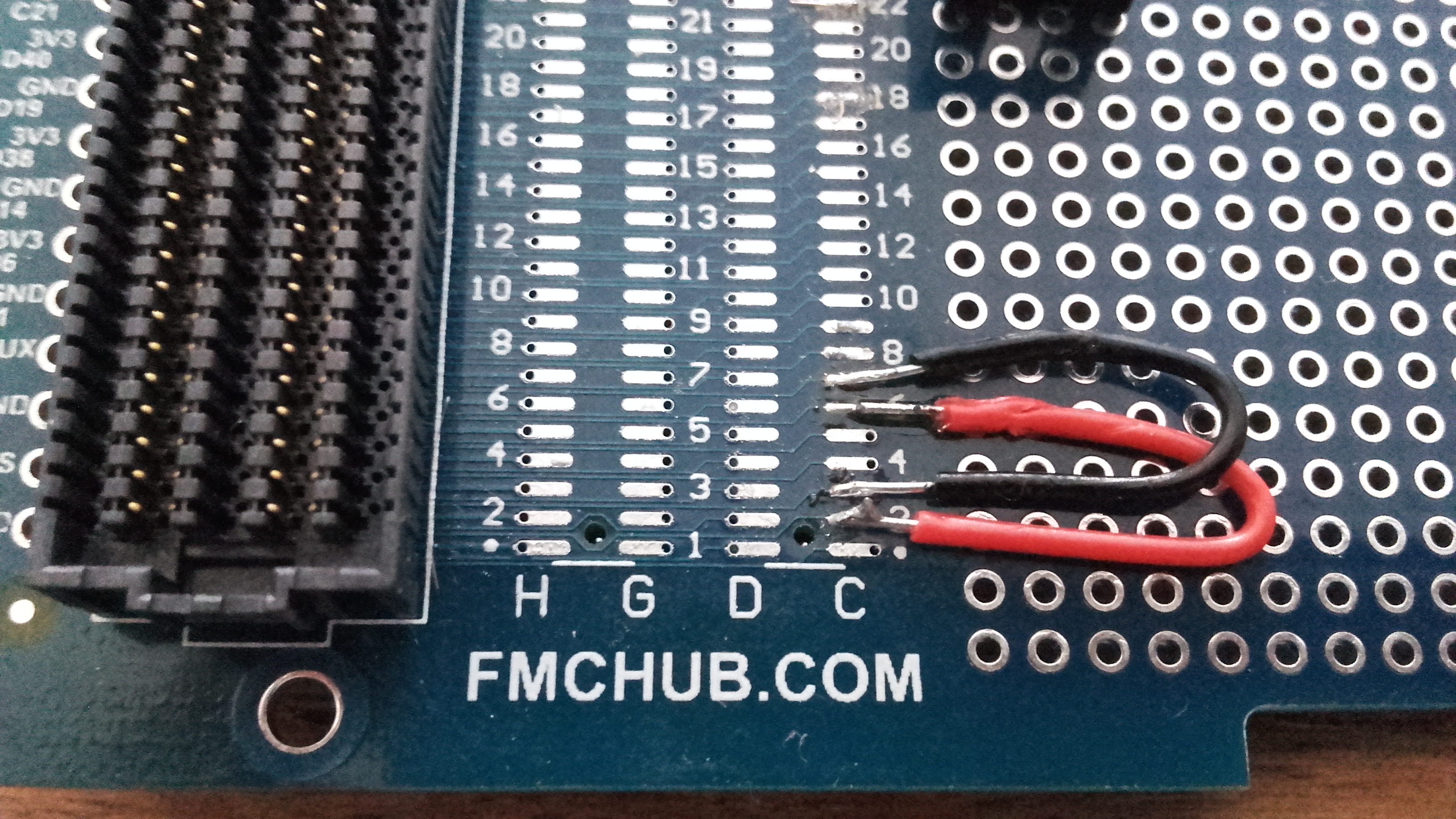
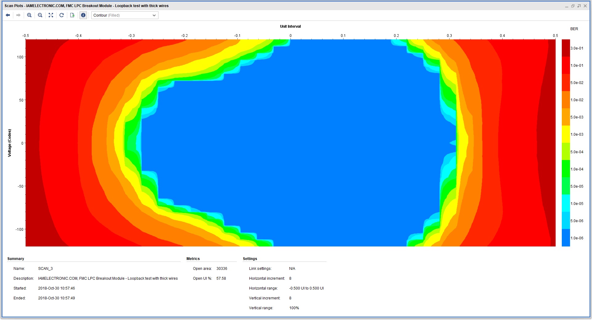
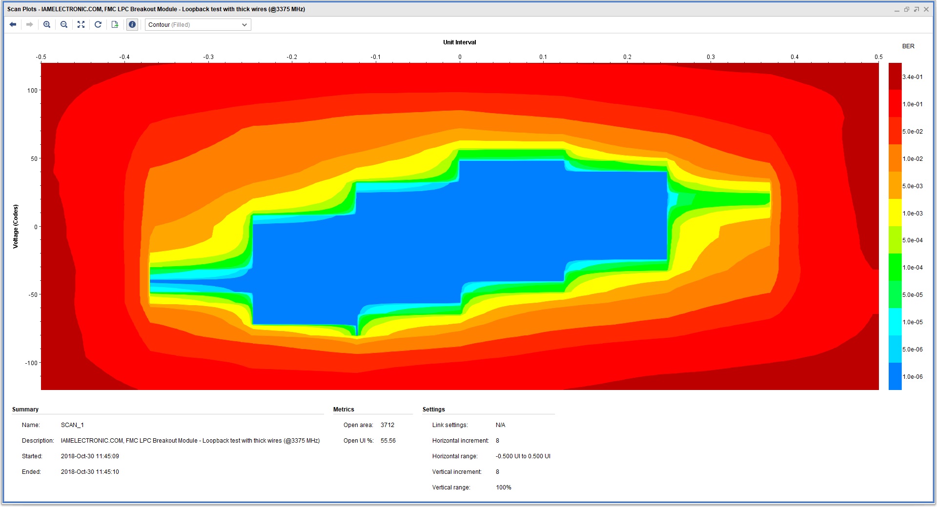
4. Loopback testing For the implementation of high-speed data links with FPGAs, loopback testing is a useful method for evaluating performance of the carrier platform and verifying the FPGA design. The FMC LPC Breakout Module can be hooked up as loopback device by shorting the appropriate pins on the board. We have checked different soldered wire connections at two line rates (1350 MHz and 3375 MHz) with Xilinx IBERT core on Xilinx Artix-7 FPGA (XC7A200T-1SBG484C). All the loose cable connections from Tab. 1 were capable of transmitting pseudorandom binary sequence pattens (7-bit PRBS pattern) at the tested data rates without any errors.
Tab. 1: FMC LPC Breakout Module with different soldered wire connections for shorting the loopback. The eye scans were recorded with Xilinx IBERT core for GTP transceivers on a Artix-7 FPGA (XC7A200T-1SBG484C).| Soldered wire connection | Eye scan at 1.350 GHz | Eye scan at 3.375 GHz |
 |
 |
 |
 |
 |
 |
 |
 |
 |
General information
Depending on the application, it is recommended to solder additional pin headers to the power pin array and to the breakout pad array. Standard
pin headers are suitable and fit the PCB layout.
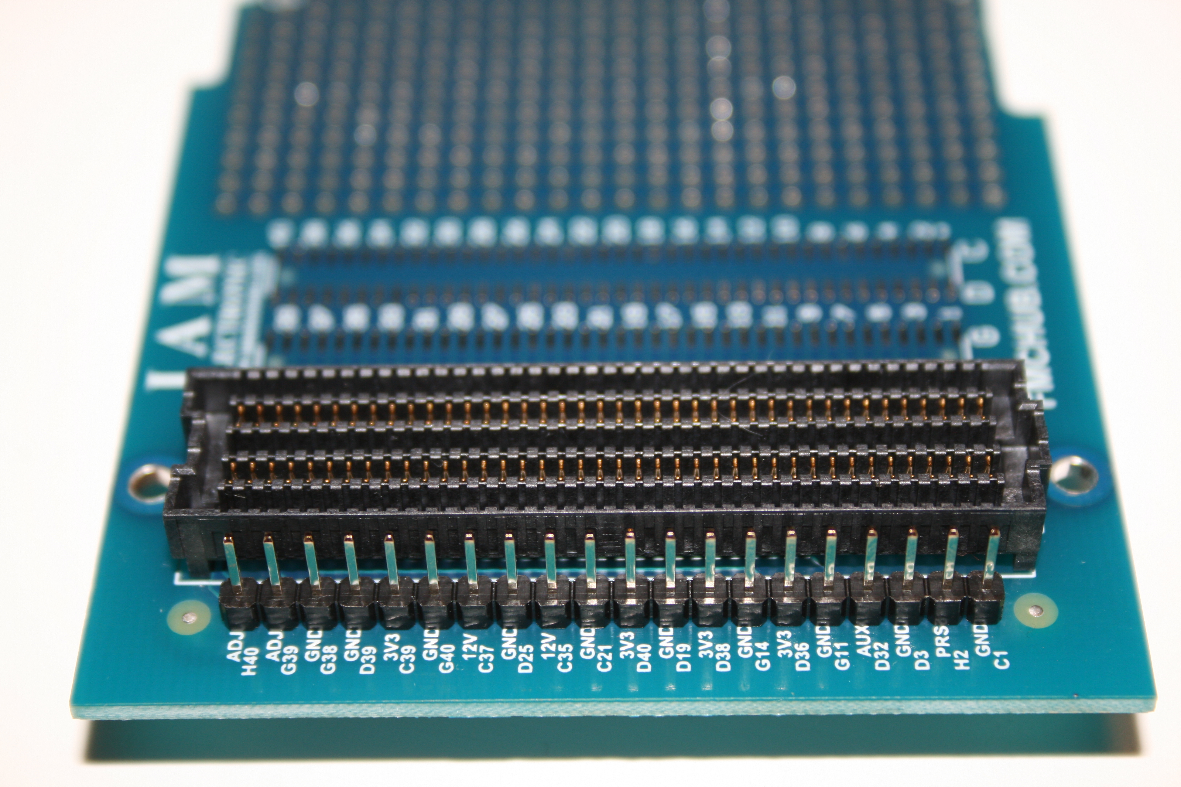 Fig. 2: FMC LPC Breakout module with separate power vias and equipped pin headers (20 pos., 2.54 mm pitch).
The printed circuit board is open-source hardware! You can download the FMC LPC breakout board schematics and PCB layout files in their latest revision from http://www.fmchub.com. The parts list (see tab. 1) is very simple, because it consists of only two parts. Tab. 2: Parts list of the FMC LPC Breakout board.
| FMC connector | Samtec part no. | Molex part no. | Description |
| 1. CC-LPC-10 | ASP-134603-01 | 45971-4305 | female, baseboard side, Low-pin count (LPC), 160 I/O, tin-lead |
| 2. MC-LPC-10 | ASP-134604-01 | 45970-4305 | male, mezzanine card side, Low-pin count (LPC), 160 I/O, lead-free, 10 mm mated stack height |
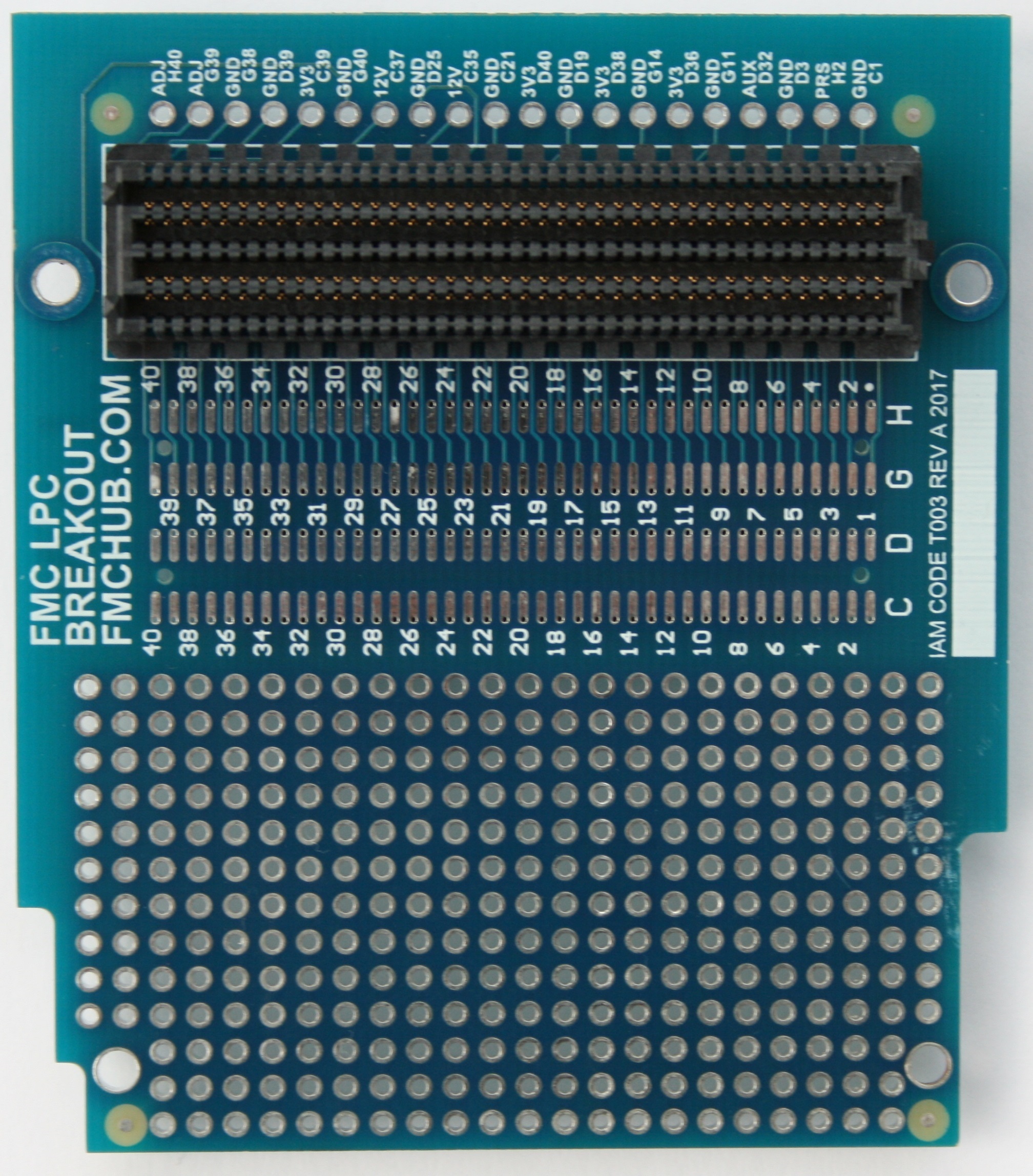
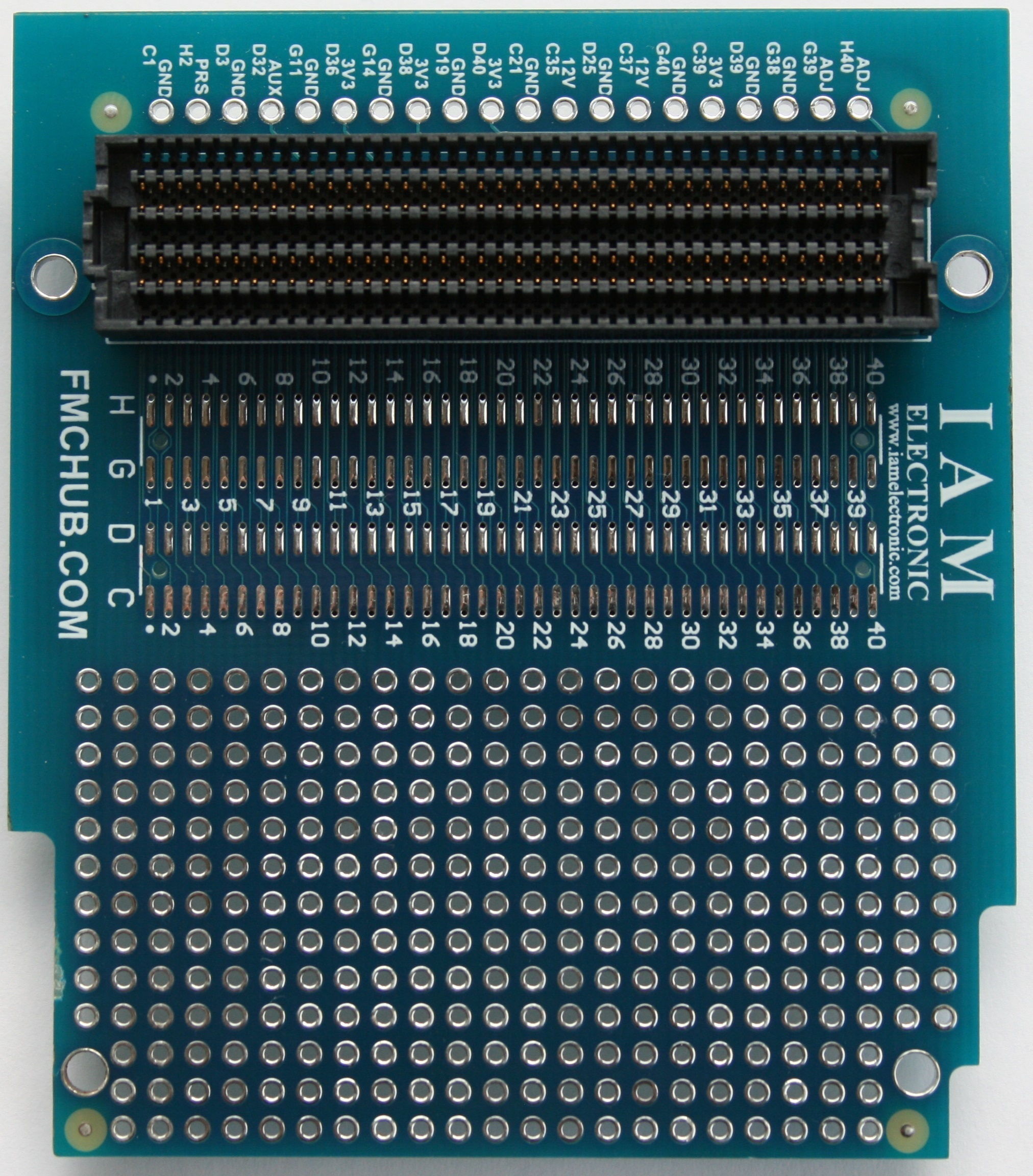
The ANSI/VITA 57.1 FMC standard describes different power supply pins on the LPC connector. The most important are routed to a separate via row next to the FMC connector in the back of the module (see fig. 3).
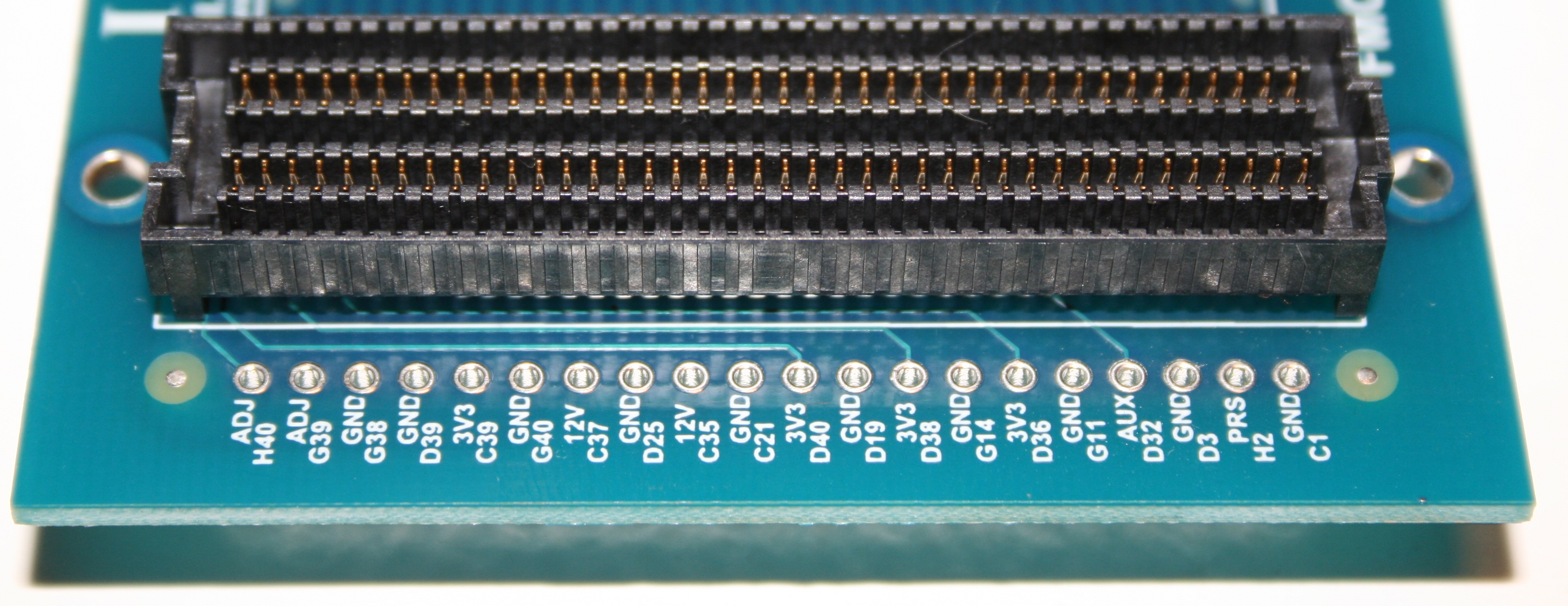 Fig. 3: FMC LPC Breakout board with separate power vias (2.54 mm pitch).
A list of the power supply pins provided by the via row is shown in tab. 2.
Tab. 3: Power pin vias and their signal names, locations, and trace widths on the PCB.
Fig. 3: FMC LPC Breakout board with separate power vias (2.54 mm pitch).
A list of the power supply pins provided by the via row is shown in tab. 2.
Tab. 3: Power pin vias and their signal names, locations, and trace widths on the PCB.
| Signal name | Source | Destination | Trace width |
| VADJ | H40 | Power Via #1 | 0.254 mm (10 mil) |
| VADJ | G39 | Power Via #2 | 0.254 mm (10 mil) |
| GND | G38 | Power Via #3 | 0.254 mm (10 mil) |
| GND | D39 | Power Via #4 | 0.254 mm (10 mil) |
| 3P3V | C39 | Power Via #5 | 0.254 mm (10 mil) |
| GND | G40 | Power Via #6 | 0.254 mm (10 mil) |
| 12P0V | C37 | Power Via #7 | 0.254 mm (10 mil) |
| GND | D25 | Power Via #8 | 0.254 mm (10 mil) |
| 12P0V | C35 | Power Via #9 | 0.254 mm (10 mil) |
| GND | C21 | Power Via #10 | 0.254 mm (10 mil) |
| 3P3V | D40 | Power Via #11 | 0.254 mm (10 mil) |
| GND | D19 | Power Via #12 | 0.254 mm (10 mil) |
| 3P3V | D38 | Power Via #13 | 0.254 mm (10 mil) |
| GND | G14 | Power Via #14 | 0.254 mm (10 mil) |
| 3P3V | D36 | Power Via #15 | 0.254 mm (10 mil) |
| GND | G11 | Power Via #16 | 0.254 mm (10 mil) |
| 3P3VAUX | D32 | Power Via #17 | 0.254 mm (10 mil) |
| GND | D3 | Power Via #18 | 0.254 mm (10 mil) |
| PRSNT_M2C_L | H2 | Power Via #19 | 0.254 mm (10 mil) |
| GND | C1 | Power Via #20 | 0.254 mm (10 mil) |
The signals from the LPC connector are routed to an array of pads (fig. 4).
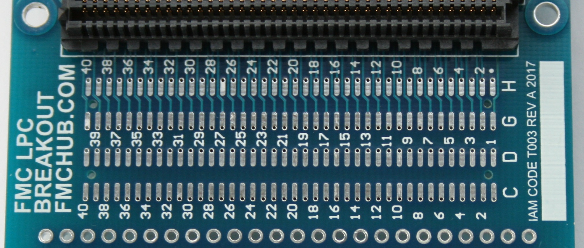 Fig. 4: FMC LPC Breakout board with an array of pads (1.27 mm pitch) for general purpose access to ANSI/VITA 57.1 signals.
Tab. 4: Signals of the ANSI/VITA 57.1 FMC LPC connector and pad array.
Fig. 4: FMC LPC Breakout board with an array of pads (1.27 mm pitch) for general purpose access to ANSI/VITA 57.1 signals.
Tab. 4: Signals of the ANSI/VITA 57.1 FMC LPC connector and pad array.
| Pin # | Row H | Row G | Row D | Row C |
| 1 | VREF_A_M2C | GND | PG_C2M | GND |
| 2 | PRSNT_M2C_L | CLK1_M2C_P | GND | DP0_C2M_P |
| 3 | GND | CLK1_M2C_N | GND | DP0_C2M_N |
| 4 | CLK0_M2C_P | GND | GBTCLK0_M2C_P | GND |
| 5 | CLK0_M2C_N | GND | GBTCLK0_M2C_N | GND |
| 6 | GND | LA00_P_CC | GND | DP0_M2C_P |
| 7 | LA02_P | LA00_N_CC | GND | DP0_M2C_N |
| 8 | LA02_N | GND | LA01_P_CC | GND |
| 9 | GND | LA03_P | LA01_N_CC | GND |
| 10 | LA04_P | LA03_N | GND | LA06_P |
| 11 | LA04_N | GND | LA05_P | LA06_N |
| 12 | GND | LA08_P | LA05_N | GND |
| 13 | LA07_P | LA08_N | GND | GND |
| 14 | LA07_N | GND | LA09_P | LA10_P |
| 15 | GND | LA12_P | LA09_N | LA10_N |
| 16 | LA11_P | LA12_N | GND | GND |
| 17 | LA11_N | GND | LA13_P | GND |
| 18 | GND | LA16_P | LA13_N | LA14_P |
| 19 | LA15_P | LA16_N | GND | LA14_N |
| 20 | LA15_N | GND | LA17_P_CC | GND |
| 21 | GND | LA20_P | LA17_N_CC | GND |
| 22 | LA19_P | LA20_N | GND | LA18_P_CC |
| 23 | LA19_N | GND | LA23_P | LA18_N_CC |
| 24 | GND | LA22_P | LA23_N | GND |
| 25 | LA21_P | LA22_N | GND | GND |
| 26 | LA21_N | GND | LA26_P | LA27_P |
| 27 | GND | LA25_P | LA26_N | LA27_N |
| 28 | LA24_P | LA25_N | GND | GND |
| 29 | LA24_N | GND | TCK | GND |
| 30 | GND | LA29_P | TDI | SCL |
| 31 | LA28_P | LA29_N | TDO | SDA |
| 32 | LA28_N | GND | 3P3VAUX | GND |
| 33 | GND | LA31_P | TMS | GND |
| 34 | LA30_P | LA31_N | TRST_L | GA0 |
| 35 | LA30_N | GND | GA1 | 12P0V |
| 36 | GND | LA33_P | 3P3V | GND |
| 37 | LA32_P | LA33_N | GND | 12P0V |
| 38 | LA32_N | GND | 3P3V | GND |
| 39 | GND | VADJ | GND | 3P3V |
| 40 | VADJ | GND | 3P3V | GND |
Please note that all Ground pins on the FMC LPC Breakout board are not tied together. This also applies to all other pins with identical function on the connector. Traces from the LPC connector to the breakout pads have a minimum width of 0.127 mm (5 mil).
The board outline is defined by ANSI/VITA 57.1 standard for single width FMC modules. The board includes region 2 and region 3 of that standard. Region 1 for additional I/O connectivity with a front panel has been omitted, such that absolute board dimensions are 78.80 mm x 69 mm. Cut outs on board shape have a radius of 1 mm. Exact dimensions are given in figure 5.
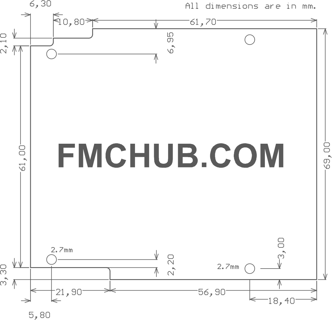 Fig. 5: Mechanical drawing of the FMC LPC breakout board.
The mounting holes are plated but have no electrical connection. Their sizes and positions are in accordance with ANSI/VITA 57.1 single width FMC modules with commercial grade mounting (air cooled).
Fig. 5: Mechanical drawing of the FMC LPC breakout board.
The mounting holes are plated but have no electrical connection. Their sizes and positions are in accordance with ANSI/VITA 57.1 single width FMC modules with commercial grade mounting (air cooled).
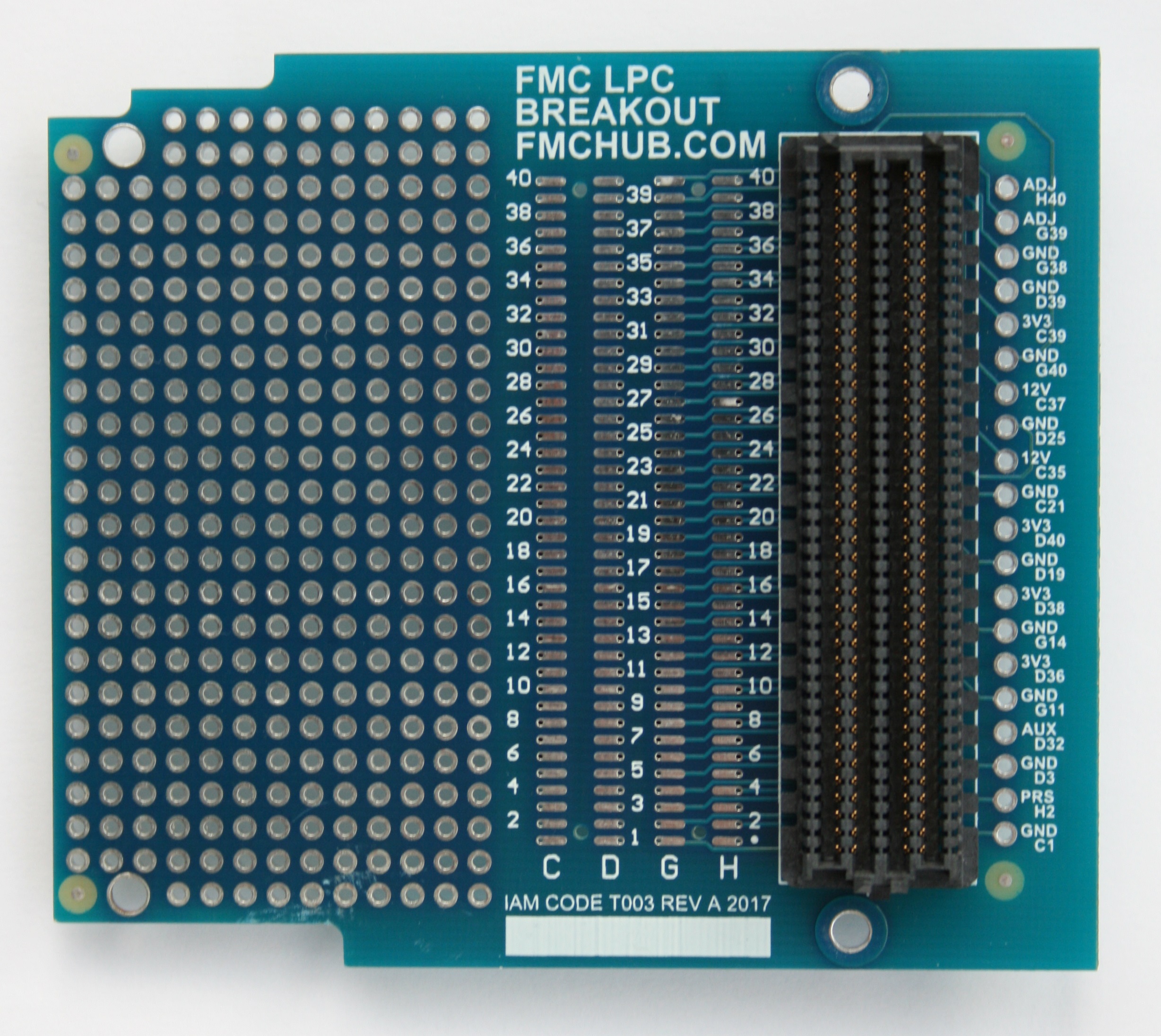 Fig. 6: Product photo of FMC LPC breakout board (bottom view).
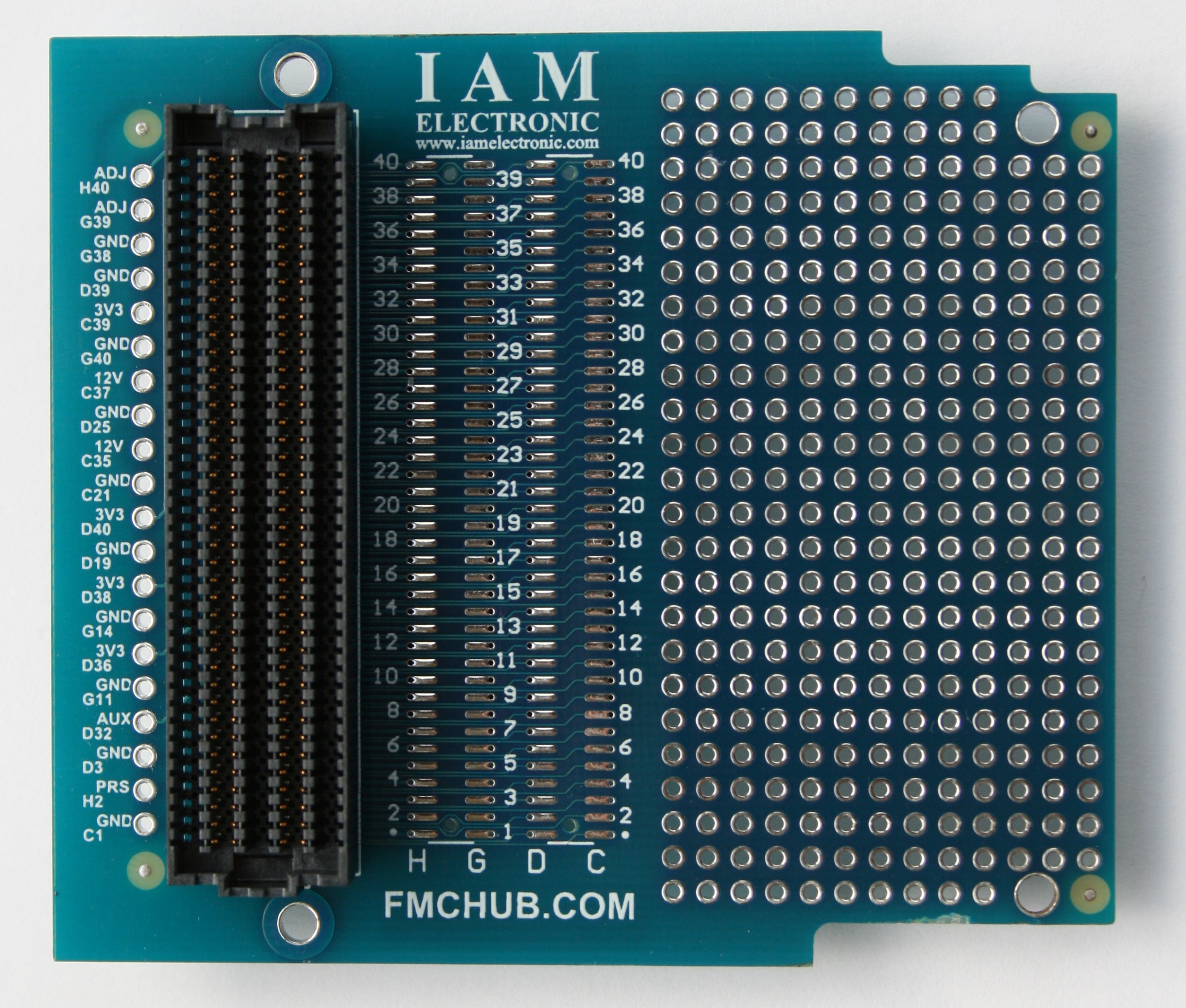 Fig. 7: Product photo of FMC LPC breakout board (top view).
| Product no. | Description | Market place | Request quote | Standard lead time |
| T0003 | FMC LPC Breakout module with bothMC-LPC-10 and CC-LPC-10 connectors on bottom and top side. | IAM Electronic Shop Ebay #183804369803 Tindie#11490 DigiKey6068-T0003-ND AmazonB0CDHJJCDC | info@iamelectronic.com | Normally in stock, otherwise 3 weeks |
| T0003MC | FMC LPC Breakout module only withMC-LPC-10 connector on bottom side. | not available (request quote) | info@iamelectronic.com | Normally in stock, otherwise 3 weeks |
| T0003CC | FMC LPC Breakout module only withCC-LPC-10 connector on top side. | not available (request quote) | info@iamelectronic.com | Normally in stock, otherwise 3 weeks |
Related products with similar or improved features |
||||
| T0017 | FMC HPC-U.FL Debug Board with both MC-HPC-10 and CC-HPC-10 connectors on bottom and top side. | IAM Electronic Shop Ebay #187227314198 Tindie#38762 DigiKey6068-T0017-ND | info@iamelectronic.com | Normally in stock, 6 weeks |
| T0018 | FMC HPC to LPC Breakout module with both MC-HPC-10 and CC-HPC-10 connectors on bottom and top side. | IAM Electronic Shop Ebay #186883255131 Tindie#37080 DigiKey6068-T0018-ND | info@iamelectronic.com | Normally in stock, 6 weeks |