- Low-pin count (LPC) connector
- Handy breakout for FMC carriers
- Pin headers with 2.54 mm pitch
- SMA connectors for high-speed data (multi gigabit transceivers)
- SMA connector for dedicated clock IO
- EEPROM for FRU information storage
- Small form factor
- Open-source hardware
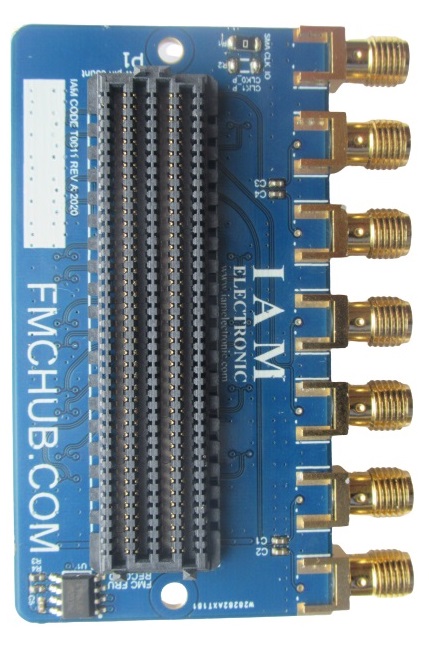
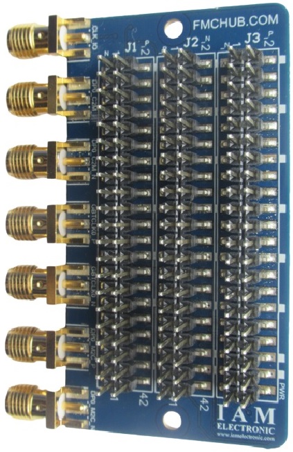
The photos below show the bottom side with LPC mezzanine card connector (MC-LPC-10) and top side with pin headers (2.54 grid) and SMA connectors.
- Easy prototyping
- Logic Analyzer
- Clock Synthesizer
- Trigger-Generator
- Pattern-Generator
- Board-to-Board interconnections
- Debugging and test of digital designs
- Research and education with FPGAs
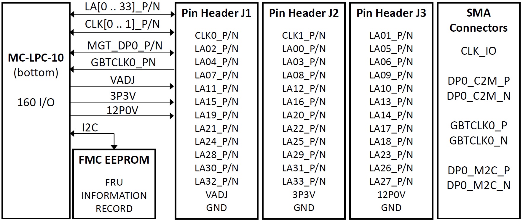
The FMC pin header board was developed to make the high density FMC connector of many FPGA boards easily accessible. In many applications easily pluggable connections are required to process and check the digital signals. The use of 2.54 mm pin headers is very common. Thus, the FMC pin header board enables a variety of applications for digital signal processing and testing. The total number of 68 user signals (LAxx_P/N), 4 user clocks (CLKx_M2C_P/N) and 3 voltage rails (VADJ, 3P3V and 12PV0) from the carrier card connector are routed to the 2.54 mm pin grid on top of the adapter board. In addition, the high-speed data lanes (multi-gigabit transceivers) are easily accessible via SMA connectors on the edge of the PCB. Finally, the board allows complete interconnection of all signals from the FMC connector.
Fig. 1 shows a typical application of the FMC pin header adapter where two carrier boards are connected together. Loose cables can be used for digital signals in the range of several 10 MHz.
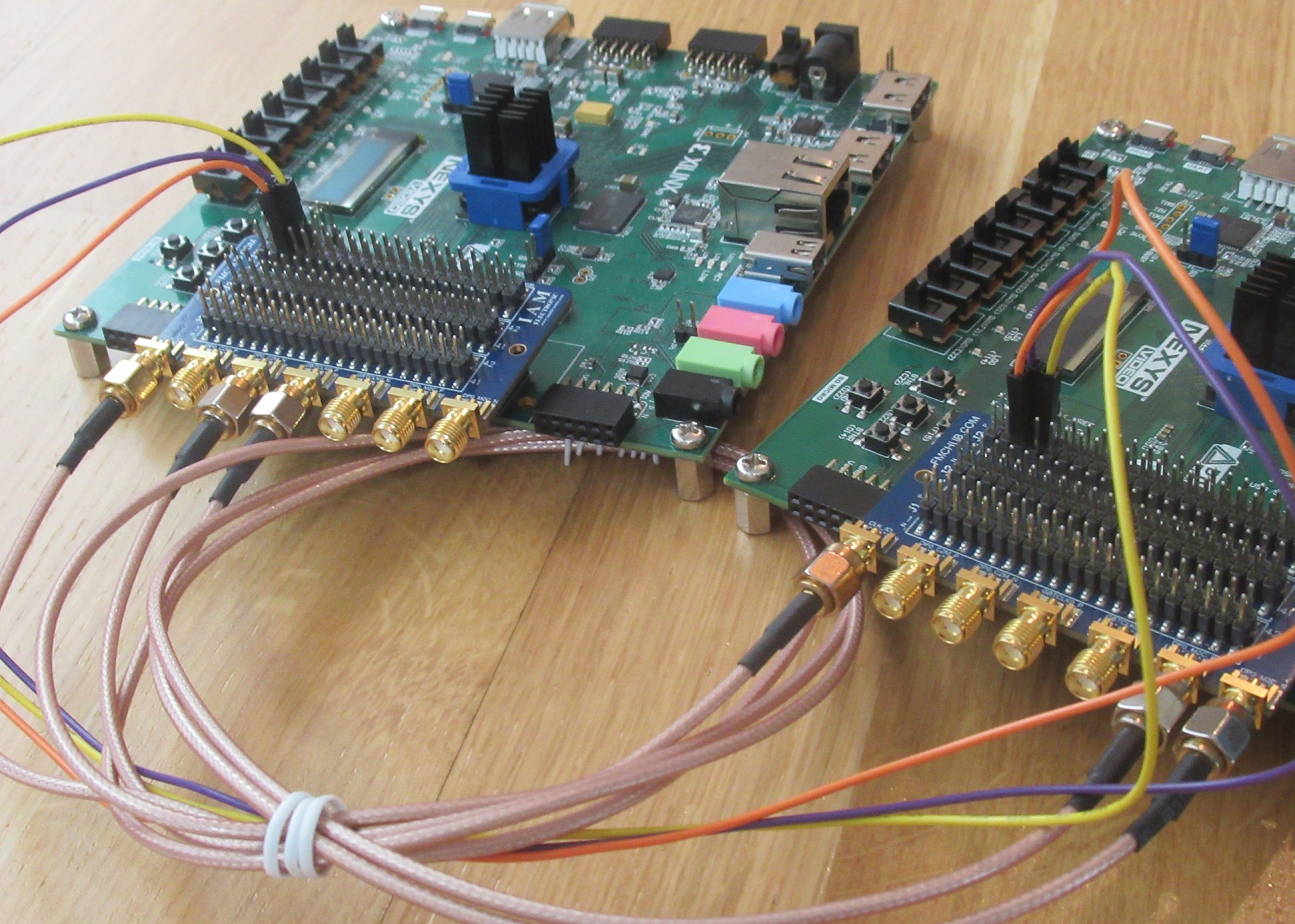 Fig. 1: Board-to-board interconnection with the FMC LPC pin header board.
For high-speed data connections between two boards, the SMA connectors should be used. Data rates of several gigabits per second are common and depend on the FPGA of the carrier board.
Fig. 2 below shows the test setup for measuring the maximum datarates of the Pin-Header Board with a loopback configuration. The SMA cables are about 50 cm long.
Fig. 1: Board-to-board interconnection with the FMC LPC pin header board.
For high-speed data connections between two boards, the SMA connectors should be used. Data rates of several gigabits per second are common and depend on the FPGA of the carrier board.
Fig. 2 below shows the test setup for measuring the maximum datarates of the Pin-Header Board with a loopback configuration. The SMA cables are about 50 cm long.
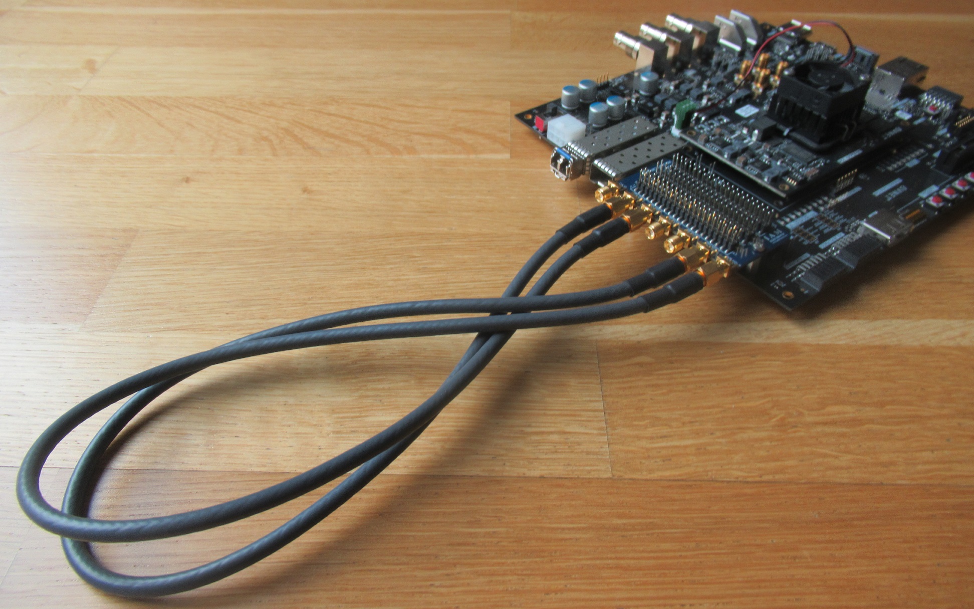 Fig. 2: Loopback connection with the FMC LPC pin header board.
The SMA connectors of the Pin Header Board have been tested with datarates up to 8.5 Gbps without
errors. Even faster connections are possible, but then the cable quality and length are more important than the characteristics of the board itself.
Fig. 3 and fig. 4 show the results of an eyescan with an Xilinx Zynq Ultrascale+ FPGA.
Fig. 2: Loopback connection with the FMC LPC pin header board.
The SMA connectors of the Pin Header Board have been tested with datarates up to 8.5 Gbps without
errors. Even faster connections are possible, but then the cable quality and length are more important than the characteristics of the board itself.
Fig. 3 and fig. 4 show the results of an eyescan with an Xilinx Zynq Ultrascale+ FPGA.
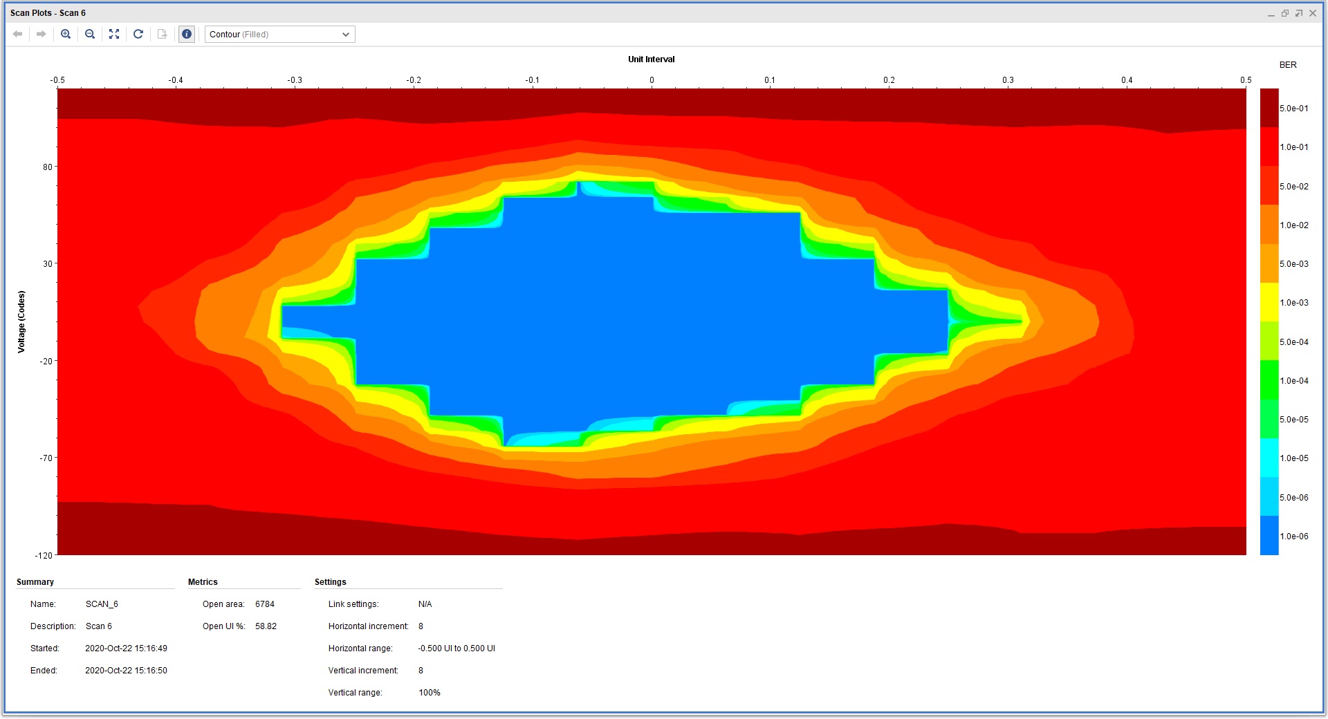 Fig. 3: Eyescan of the loopback connection with a datarate of 5.94 Gbps.
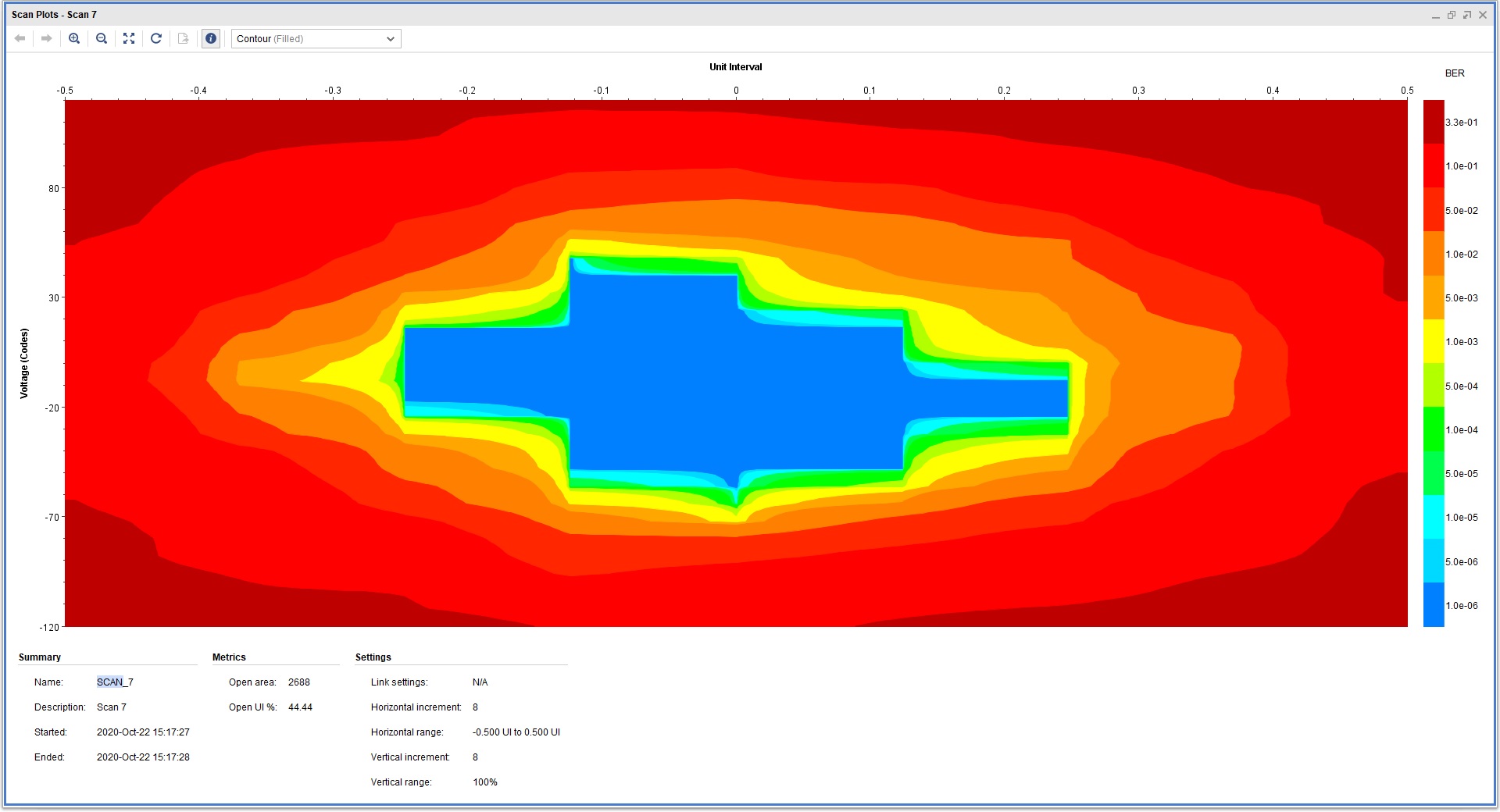 Fig. 4: Eyescan of the loopback connection with a datarate of 8.5 Gbps.
The printed circuit board is open-source hardware! You can download the FMC LPC pinheader board schematics and PCB layout files in their latest revision from http://www.fmchub.com.
3.1 Pinout of the 2.54 mm pin headers
Fig. 5 and tab. 1 show the connections of the FMC signals on the pin header connectors J1, J2, and J3.
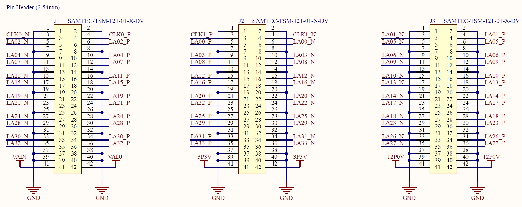 Fig. 5: Pin assignments of the FMC LPC pins to the pin headers J1, J2, and J3.
| FMC pin name | FMC pin designator | Pin Header | Pin number |
| LA00_P_CC | G6 | J2 | 5 |
| LA00_N_CC | G7 | J2 | 6 |
| LA01_N_CC | D9 | J3 | 3 |
| LA01_P_CC | D8 | J3 | 4 |
| LA02_N | H8 | J1 | 5 |
| LA02_P | H7 | J1 | 6 |
| LA03_P | G9 | J2 | 9 |
| LA03_N | G10 | J2 | 10 |
| LA04_N | H11 | J1 | 9 |
| LA04_P | H10 | J1 | 10 |
| LA05_N | D12 | J3 | 5 |
| LA05_P | D11 | J3 | 6 |
| LA06_N | C11 | J3 | 9 |
| LA06_P | C10 | J3 | 10 |
| LA07_N | H14 | J1 | 11 |
| LA07_P | H13 | J1 | 12 |
| LA08_P | G12 | J2 | 11 |
| LA08_N | G13 | J2 | 12 |
| LA09_N | D15 | J3 | 11 |
| LA09_P | D14 | J3 | 12 |
| LA10_N | C15 | J3 | 15 |
| LA10_P | C14 | J3 | 16 |
| LA11_N | H17 | J1 | 15 |
| LA11_P | H16 | J1 | 16 |
| LA12_P | G15 | J2 | 15 |
| LA12_N | G16 | J2 | 16 |
| LA13_N | D18 | J3 | 17 |
| LA13_P | D17 | J3 | 18 |
| LA14_N | C19 | J3 | 21 |
| LA14_P | C18 | J3 | 22 |
| LA15_N | H20 | J1 | 17 |
| LA15_P | H19 | J1 | 18 |
| LA16_P | G18 | J2 | 17 |
| LA16_N | G19 | J2 | 18 |
| LA17_N_CC | D21 | J3 | 23 |
| LA17_P_CC | D20 | J3 | 24 |
| LA18_N_CC | C23 | J3 | 27 |
| LA18_P_CC | C22 | J3 | 28 |
| LA19_N | H23 | J1 | 21 |
| LA19_P | H22 | J1 | 22 |
| LA20_P | G21 | J2 | 21 |
| LA20_N | G22 | J2 | 22 |
| LA21_N | H26 | J1 | 23 |
| LA21_P | H25 | J1 | 24 |
| LA22_P | G24 | J2 | 23 |
| LA22_N | G25 | J2 | 24 |
| LA23_N | D24 | J3 | 29 |
| LA23_P | D23 | J3 | 30 |
| LA24_N | H29 | J1 | 27 |
| LA24_P | H28 | J1 | 28 |
| LA25_P | G27 | J2 | 27 |
| LA25_N | G28 | J2 | 28 |
| LA26_N | D27 | J3 | 33 |
| LA26_P | D26 | J3 | 34 |
| LA27_N | C27 | J3 | 35 |
| LA27_P | C26 | J3 | 36 |
| LA28_N | H33 | J1 | 29 |
| LA28_P | H31 | J1 | 30 |
| LA29_P | G30 | J2 | 29 |
| LA29_N | G31 | J2 | 30 |
| LA30_N | H35 | J1 | 33 |
| LA30_P | H34 | J1 | 34 |
| LA31_P | G33 | J2 | 33 |
| LA31_N | G34 | J2 | 34 |
| LA32_N | H38 | J1 | 35 |
| LA32_P | H37 | J1 | 36 |
| LA33_P | G36 | J2 | 35 |
| LA33_N | G37 | J2 | 36 |
| CLK0_P | H4 | J1 | 4 |
| CLK0_N | H5 | J1 | 3 |
| CLK1_P | G2 | J2 | 3 |
| CLK1_N | G3 | J2 | 4 |
| DP0_C2M_P | C2 | SMA | 6 |
| DP0_C2M_N | C3 | SMA | 5 |
| DP0_M2C_P | C6 | SMA | 2 |
| DP0_M2C_N | C7 | SMA | 1 |
| GBTCLK0_M2C_P | D4 | SMA | 4 |
| GBTCLK0_M2C_N | D5 | SMA | 3 |
| CLK0_M2C_P / CLK1_M2C_P | H4 / G2 | SMA | 7 |
3.2 SMA Connectors for Gigabit transceivers
The FMC LPC connector has one multi-gigabit transceiver data pair (DP0_M2C_P/N and DP0_M2C_P/N) and a corresponding differential clock input (GBTCLK0_M2C_P/N).
These six signals are all routed to the SMA connectors. The circuitry is shown in Fig. 6.
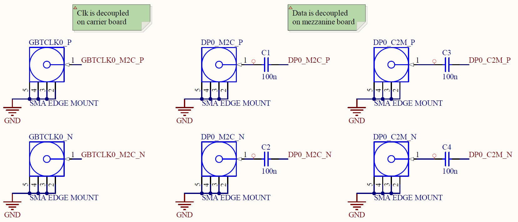 Fig. 6: SMA connectors with corresponding Gigabit transceiver ports on the FMC connector (schematic view).
Fig. 7 shows the signal assignemnts, but the designators of the signals can be also read on the circuit board..
Fig. 6: SMA connectors with corresponding Gigabit transceiver ports on the FMC connector (schematic view).
Fig. 7 shows the signal assignemnts, but the designators of the signals can be also read on the circuit board..
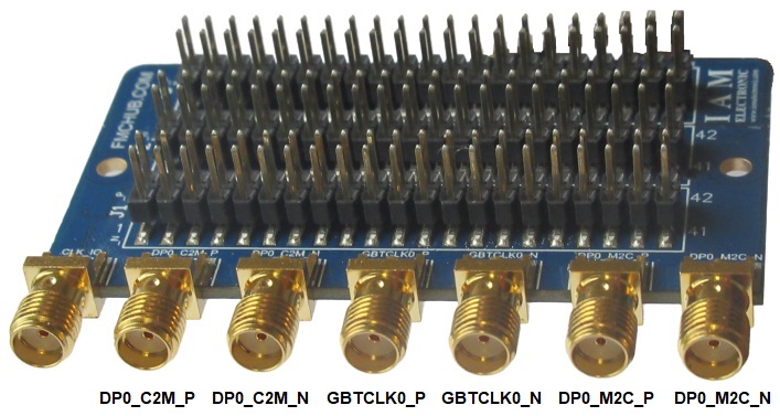 Fig. 7: SMA connectors and their associated Gigabit transceiver signals.
3.3 SMA Connector for clock IO
One of the FMC connector pins CLK0_M2C_P (pin H4) or CLK1_M2C_P (pin G2) can be routed a separate SMA connector on the board edge. A zero ohm resistor determines which clock signal will be used.
The clock signals are also routed to the 2.54 mm pin headers J1 and J2. By default, the signal CLK0_M2C_P (CLK0_P) is selected by resistor R1 (see fig. 8 and fig. 9).
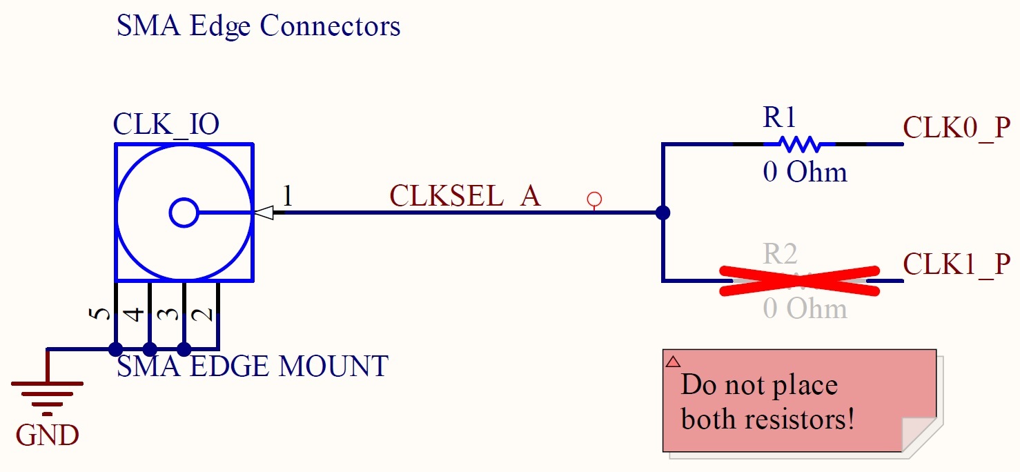 Fig. 8: Clock selection circuit with a zero ohm resistor. The SMA connector can be used as clock input or clock output.
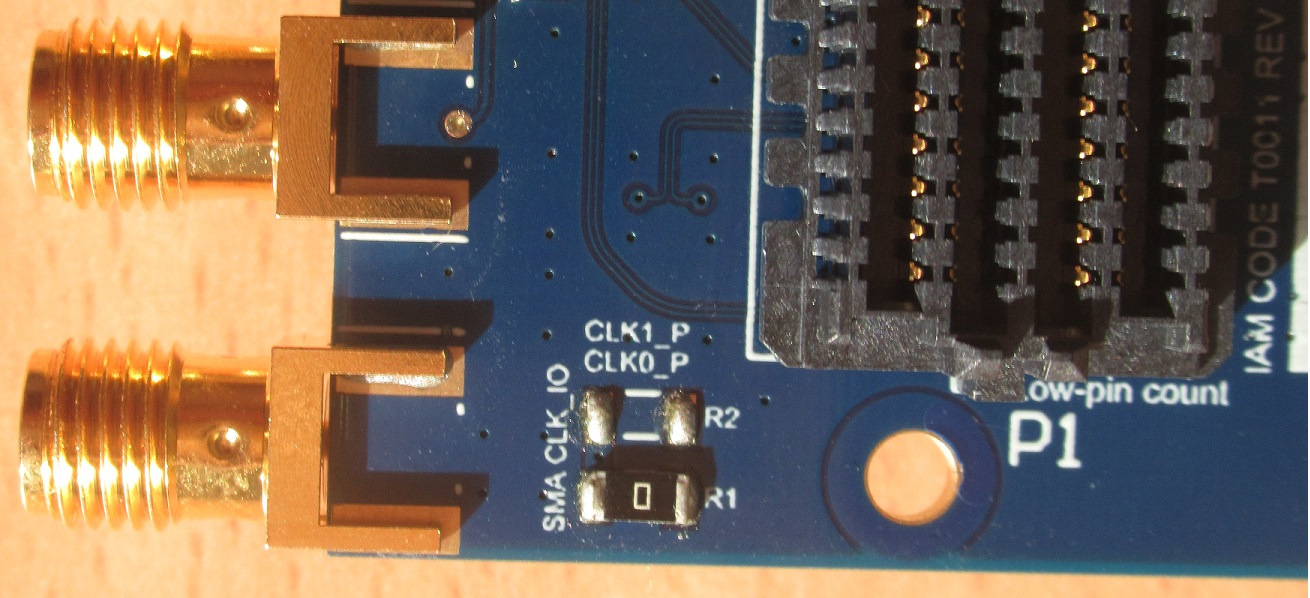 Fig. 9: Resistors R1 and R2 for selecting the clock signal CLK0_M2C_P (Pin H4) or CLK1_M2C_P (Pin G2) of the SMA connector. The size of the resistor is 1206 and can be easily soldered by hand.
The SMA connector (designator CLK_IO) for the dedicated clock signal is on the left side of the board (front view, see fig. 10).
Fig. 9: Resistors R1 and R2 for selecting the clock signal CLK0_M2C_P (Pin H4) or CLK1_M2C_P (Pin G2) of the SMA connector. The size of the resistor is 1206 and can be easily soldered by hand.
The SMA connector (designator CLK_IO) for the dedicated clock signal is on the left side of the board (front view, see fig. 10).
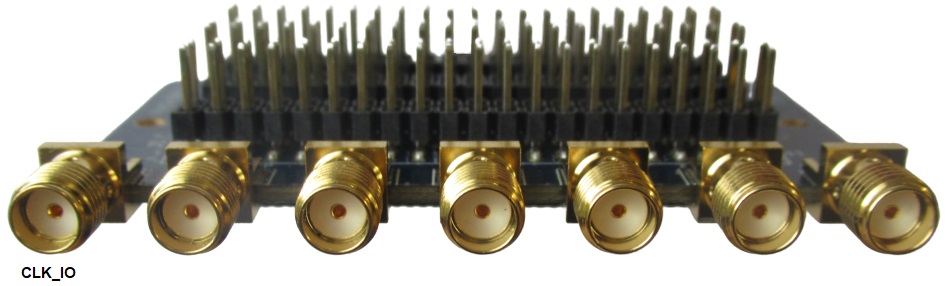 Fig. 10: The SMA connector for the dedicated clock input/output is on the left side of the board.
3.4 FMC FRU EEPROM
The EEPROM for storing FMC FRU (field replaceable unit) information is an M24C02 with 2 Kbit (256 Byte). The FRU record determines the voltage on the VADJ rail of the FMC connector.
By default, the FRU EEPROM is programmed to request 3.3 V from the carrier board. Further, the memory stores the board information such as manufacturer name and product number. The devices
can be read and written by the I2C interface of the FMC connector. The Pin Header board includes 4K7 pull-up resistors on the SCL and SDA signal lanes. The I2C address of the M24C02 is defined by
the GA0 and GA1 pins of the FMC connector in accordance with the ANSI/VITA57.1 standard.
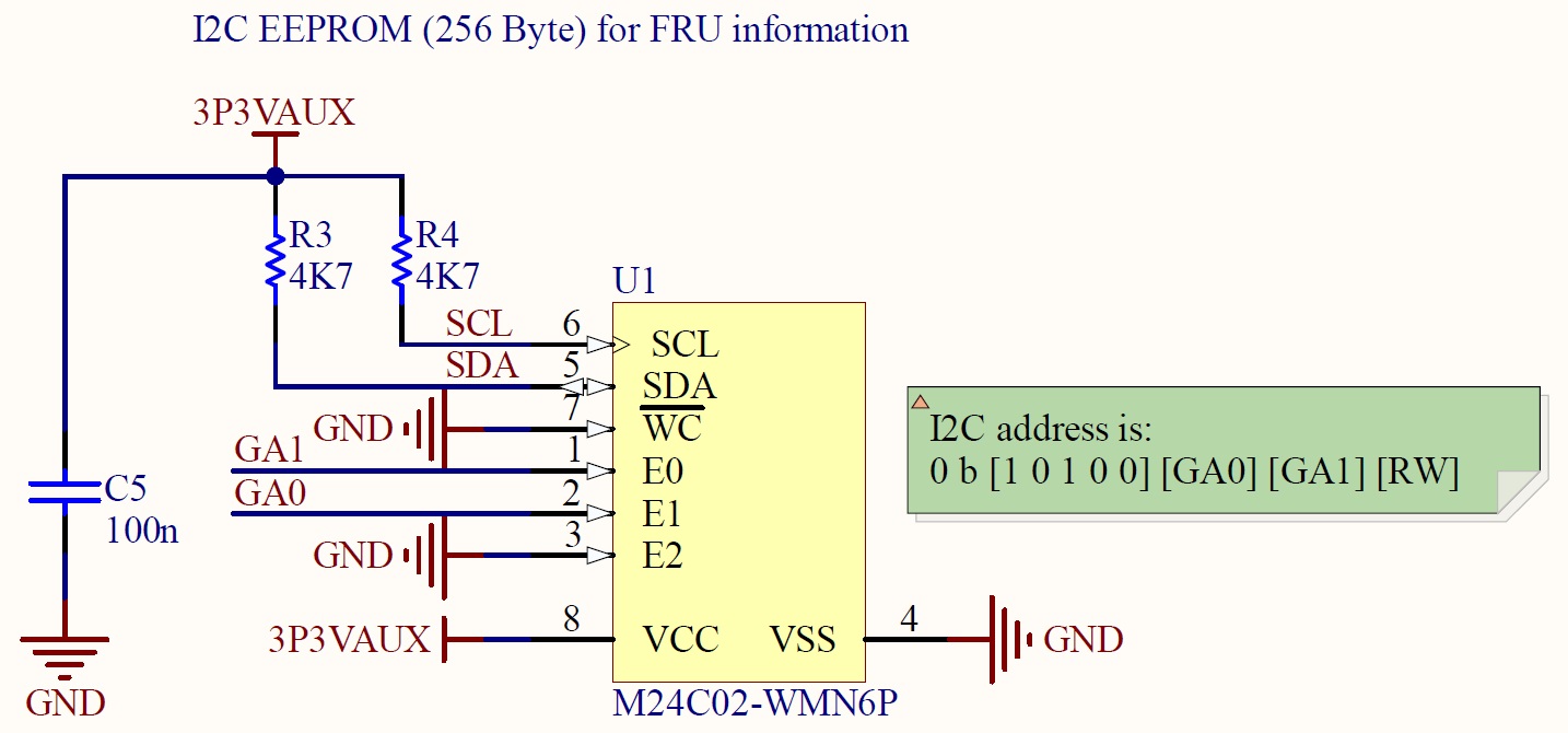
 Fig. 11: The M24C02 EEPROM stores the FMC FRU information record.
The board outline is defined by the ANSI/VITA 57.1 standard for single width FMC modules. It has a shortened length of the standard size and fits into any ANSI/VITA 57.1 compliant carrier board. The exact dimensions are given in fig. 12.
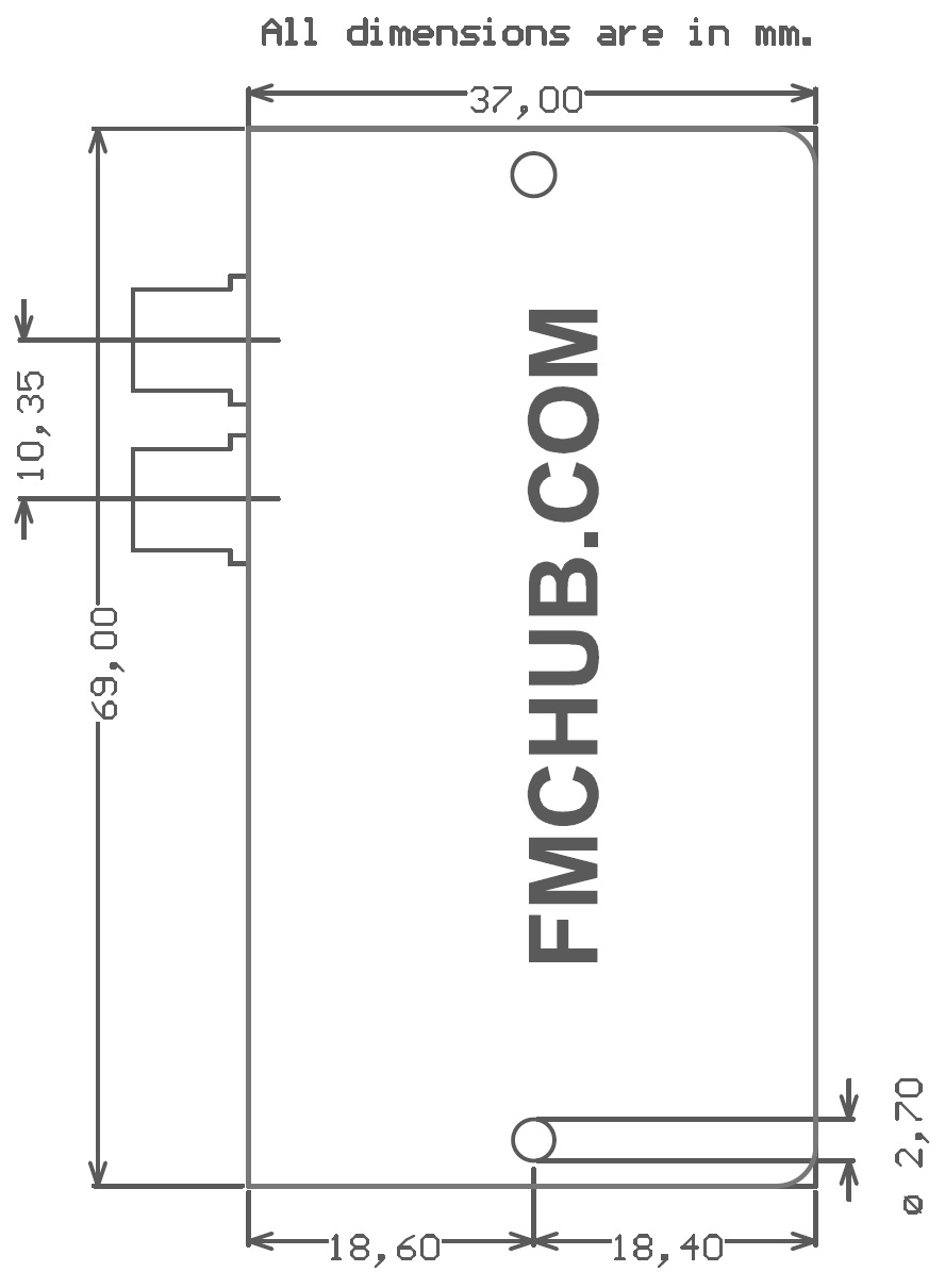 Fig. 12: Mechanical drawing of the FMC LPC Pin Header Board.
The mounting holes are plated but have no electrical connection. Their sizes and positions are in accordance with ANSI/VITA 57.1 single width FMC modules.
Fig. 12: Mechanical drawing of the FMC LPC Pin Header Board.
The mounting holes are plated but have no electrical connection. Their sizes and positions are in accordance with ANSI/VITA 57.1 single width FMC modules.
| Product no. | Description | Market place | Request quote | Standard lead time |
| T0011 | FMC LPC Pin Header Board with 2.54 mm pin headers,SMA connectors on top side, and MC-LPC-10 connector on bottom side. | IAM Electronic Shop Ebay #184517514919 Tindie#21724 DigiKey6068-T0011-ND AmazonB0CG9VXB1K | info@iamelectronic.com | Normally in stock, otherwise 3 weeks |
Related products with similar or improved features |
||||
| T0017 | FMC HPC-U.FL Debug Board with both MC-HPC-10 and CC-HPC-10 connectors on bottom and top side. | IAM Electronic Shop Ebay #187227314198 Tindie#38762 DigiKey6068-T0017-ND | info@iamelectronic.com | Normally in stock, 6 weeks |
2022/01/18: fixed pin assignments in Tab. 1 2020/11/02: Initial release