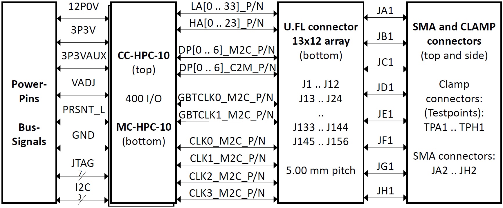
- FMC High-Pin Count (HPC) connector interface
- 156 routed signals accessible via
Hirose U.FL connectors - Up to 6 GHz signal bandwidth
- Flexible high-speed signal access via pluggable connections
- Breakout of 68 LPC LA bank signals
- Breakout of 48 HPC HA bank signals
- Breakout of 8 dedicated clock signals
- 16 differential MGT signal pairs breakout
- 8 SMA and 8 clamp probe connection points
- Stackable mechanical design
- Independent breakout of power pins
- Independent breakout of JTAG bus
- Independent breakout of JTAG bus
- Open-source hardware design
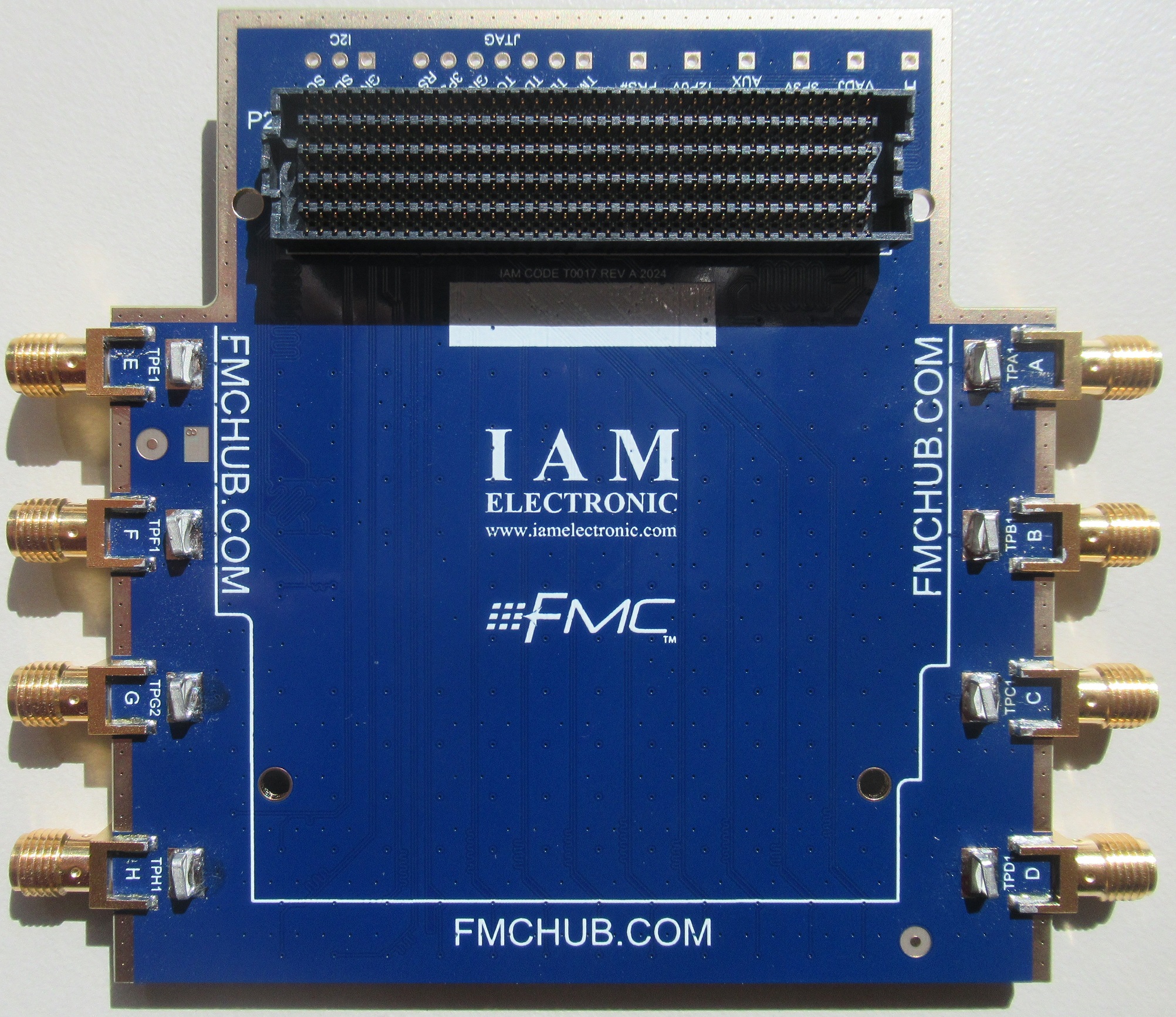
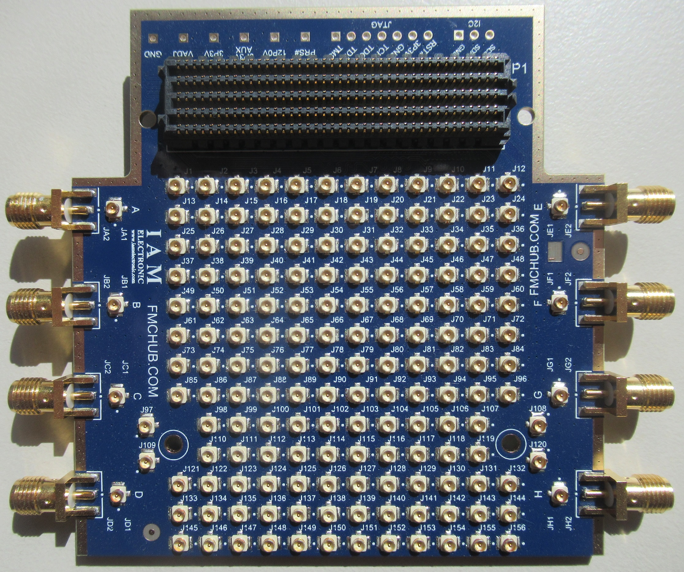
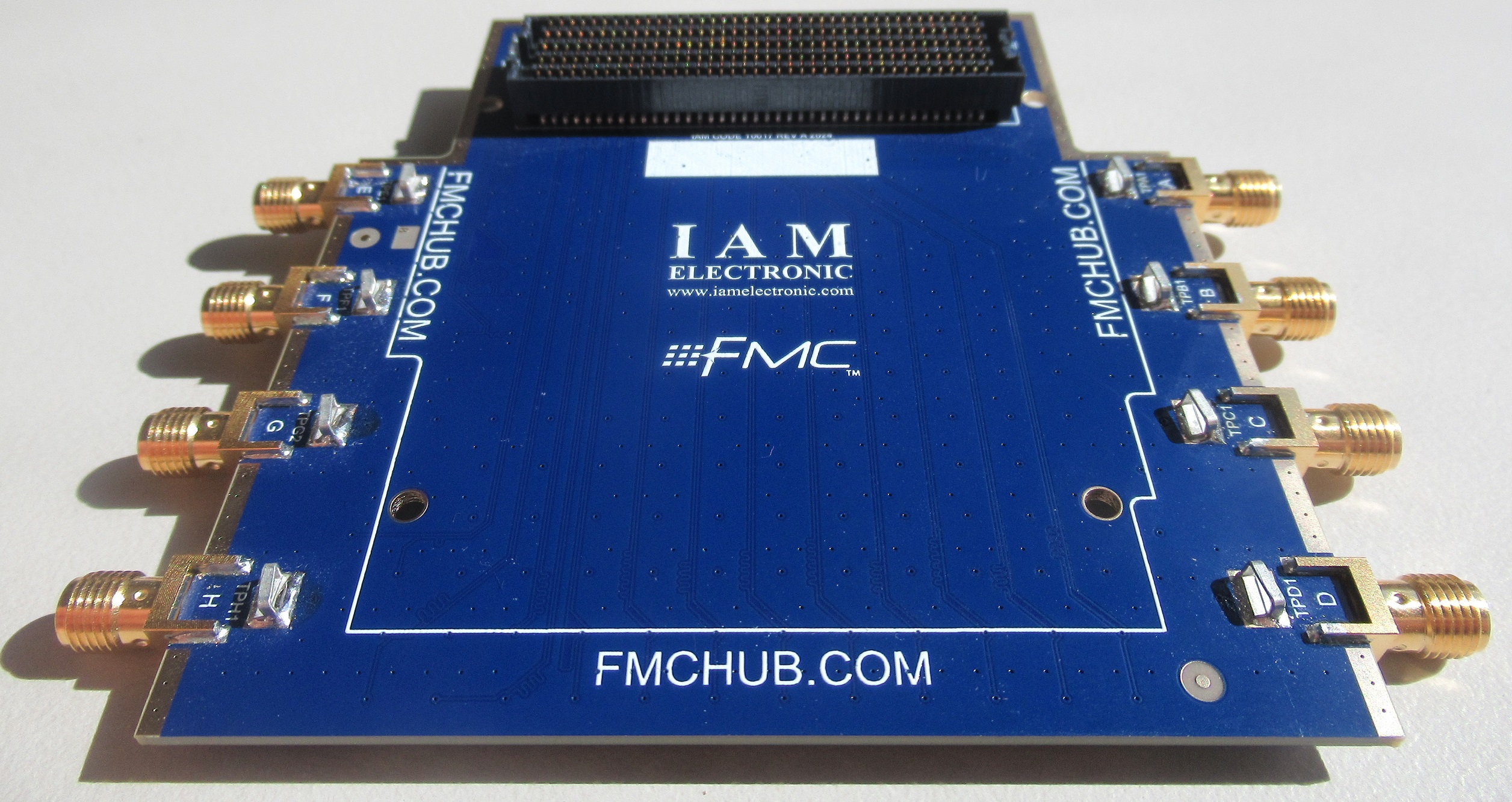
The photos below show the bottom side with HPC mezzanine card connector (MC-HPC-10) and U.FL connectors, and top side with HPC carrier card connector (CC-HPC-10) and testpoints.
- Debugging and testing of FMC modules
- Direct probing of high- and low-speed signals
- Signal loopback and board-to-board connections
- Educational use and research involving FPGAs
The FMC HPC-U.FL Debug Board is a diagnostic tool developed for use with FPGA Mezzanine Cards (FMC) utilizing the High-Pin Count (HPC) interface. The board facilitates signal access and measurement by routing key HPC signals to U.FL, SMA, and clamp connectors. This allows developers and researchers to probe, analyze, and re-route FMC signals with minimal effort and without modifying the system under test. Signal routing includes 156 U.FL-accessible signals, with breakouts for 68 LPC LA bank lines, 48 HPC HA bank lines, 8 clock signals, and 16 differential MGT pairs. The board additionally provides 8 SMA connectors and 8 clamp connection points, which can be linked to any U.FL breakout line, enabling compatibility with standard test equipment. The debug board supports a range of configurations including board-to-board and loopback setups. The mechanical design supports stackable usage, and the board includes a power breakout area for voltage monitoring and injection. It empowers developers with full flexibility to re-route and monitor signals from the FMC HPC connector, drastically simplifying the debugging process and accelerating development cycles.
The FMC HPC-U.FL Debug Board is designed to provide structured and flexible access to FPGA Mezzanine Card (FMC) signals, supporting a wide range of debugging, testing, and educational applications. Whether probing low-speed control signals or routing high-speed transceiver lanes, the board simplifies the setup and execution of complex testing scenarios. Its modular architecture and various breakout connectors (U.FL, SMA, and clamp) enable engineers to quickly reconfigure signal paths, visualize waveforms, and evaluate system performance in real time. In the following subsections, typical application use cases are explained in more detail.
2.1 Oscilloscope Probing of Low-Speed Signals For low-speed signal probing, the FMC Debug Board features 8 clamp connectors, 4 next to each other on one side. A large ground plane is exposed at the edge of the circuit board. The clamp points are intended for use with probe hooks or standard oscilloscope probe clips, enabling easy access to control, configuration, and other low-speed digital signals. They can be wired to any of the U.FL breakout points, enabling flexible selection of signals for measurement. Advantages:
- Quick and tool-less attachment of oscilloscope probes
- Ideal for control and configuration signals where signal integrity is less critical
- Safe for beginners and useful in educational environments
- Supports temporary test setups without permanent modifications
- Clamp connectors are not impedance-matched and therefore not suited for high-speed or sensitive analog signals
- Increased susceptibility to noise and interference
- Limited signal bandwidth due to connector and wiring parasitics
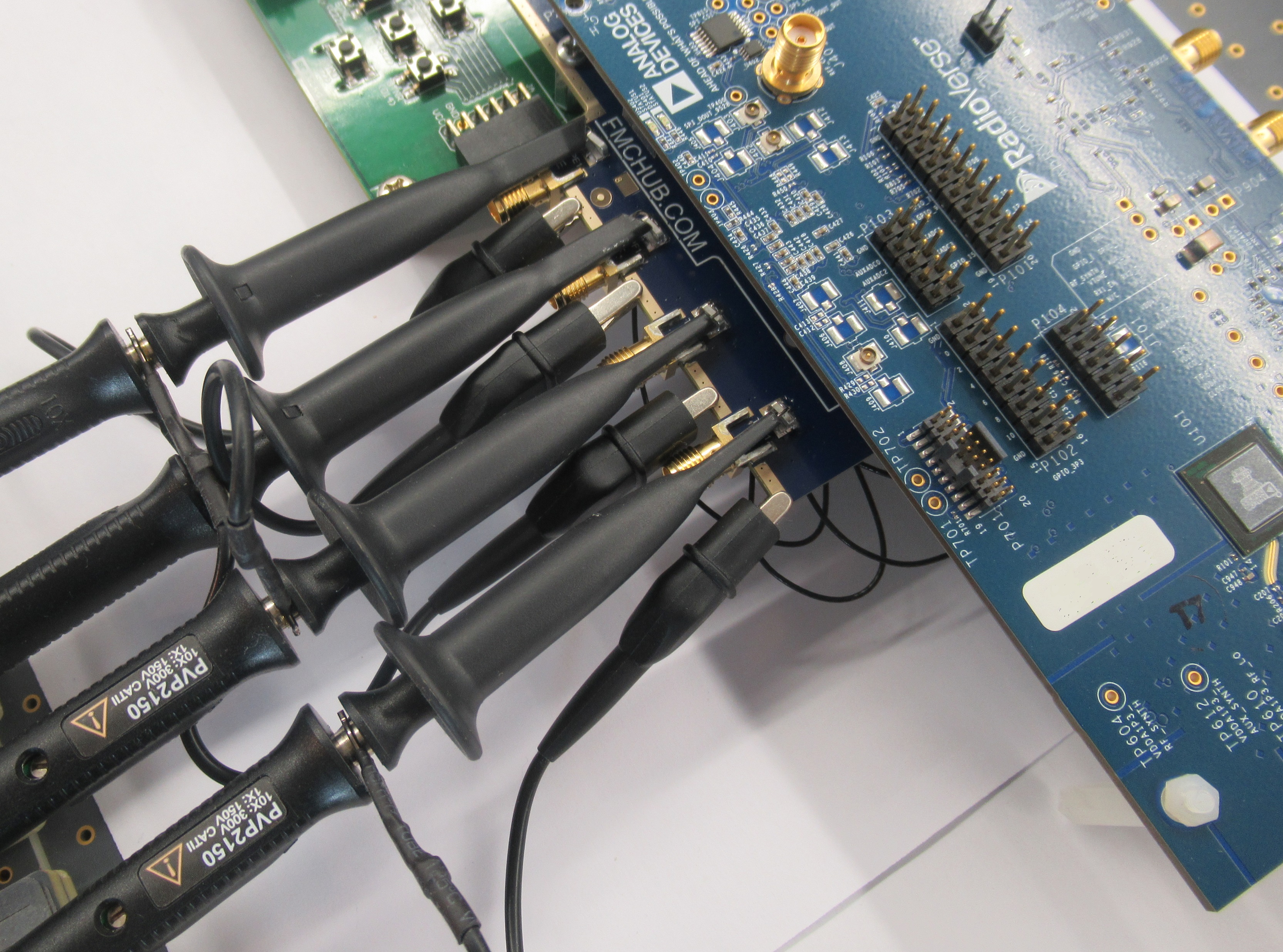 Figure 2.1: Oscilloscope probing via clamp Connectors, the FMC HPC-U.FL debug board is plugged in below the device under test.
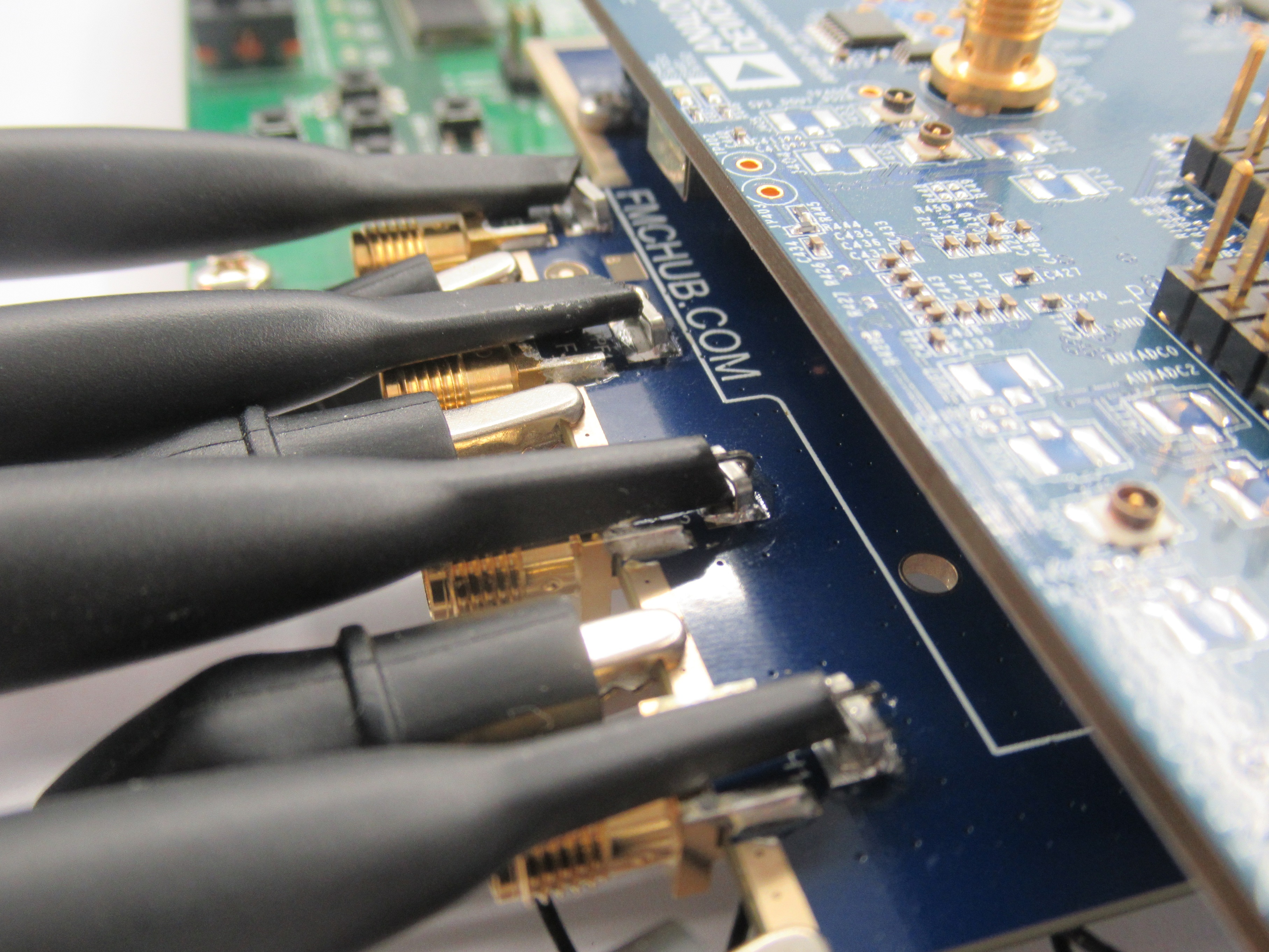 Figure 2.2: Close-up view of oscilloscope probing via clamp connectors, the FMC HPC-U.FL debug board is plugged in below the device under test.
2.2 Oscilloscope Probing of High-Speed Signals For high-speed signal measurements, the board provides 8 SMA connectors. These SMA ports can be linked to any U.FL signal using configurable jumpers or cables, allowing precise and stable access to fast differential or single-ended lines. Alternatively, high speed cables can be connected directly to the U.FL connectors (with the correct and required end-to-end connectors). Advantages:
- SMA or U.FL connectors maintain good signal integrity at high frequencies
- Secure, repeatable connections suitable for test automation
- Suitable for differential pairs, clock lines, and transceiver signals
- Compatible with high-frequency cables and test adapters
- Proper termination must be ensured to avoid reflections (e.g. 50 Ohm terminators)
- Various adapters may be needed depending on the measurement equipment
- More rigid and than probe clamps
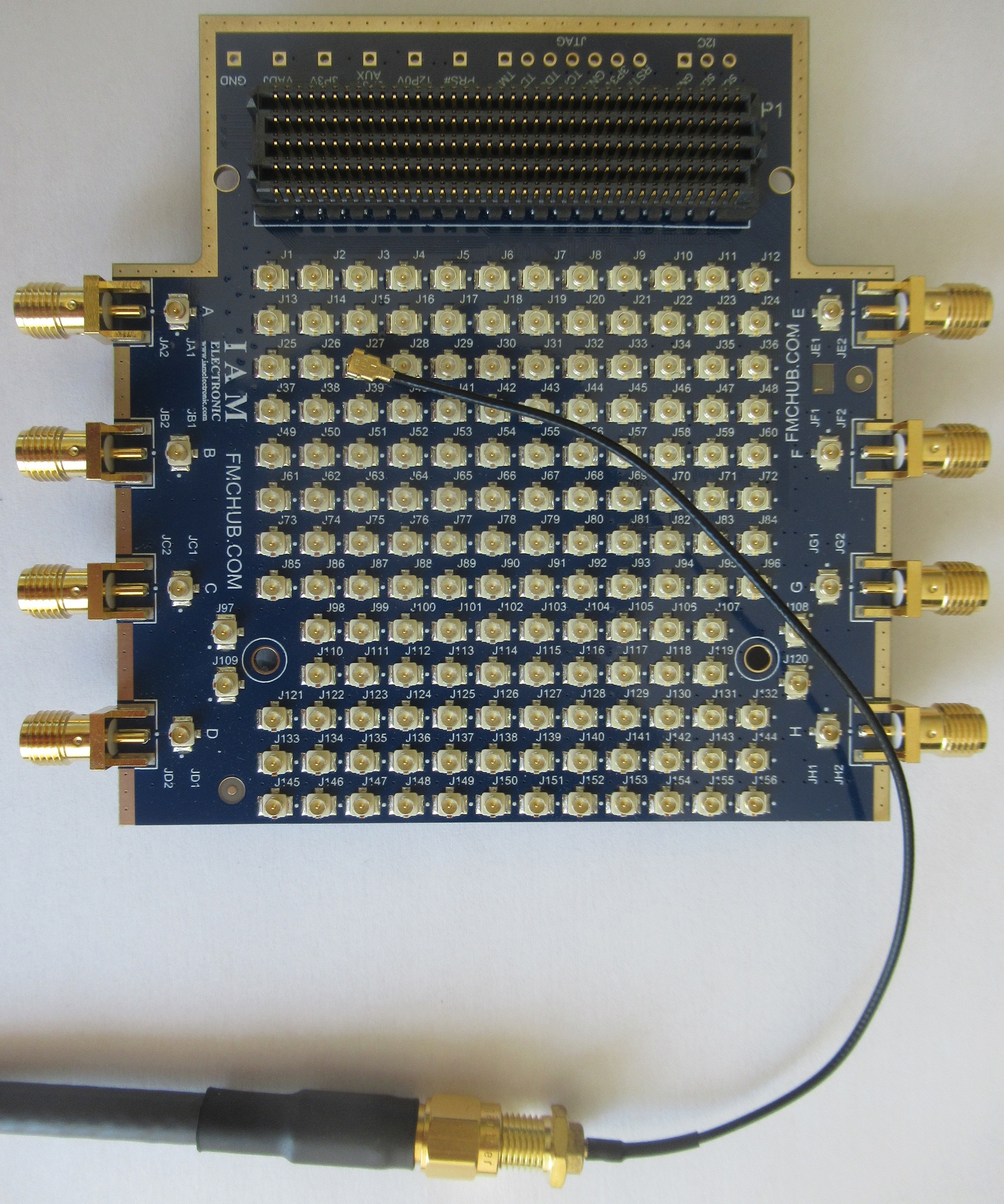 Figure 2.3: High-Speed Probing via U.FL to SMA Adapter
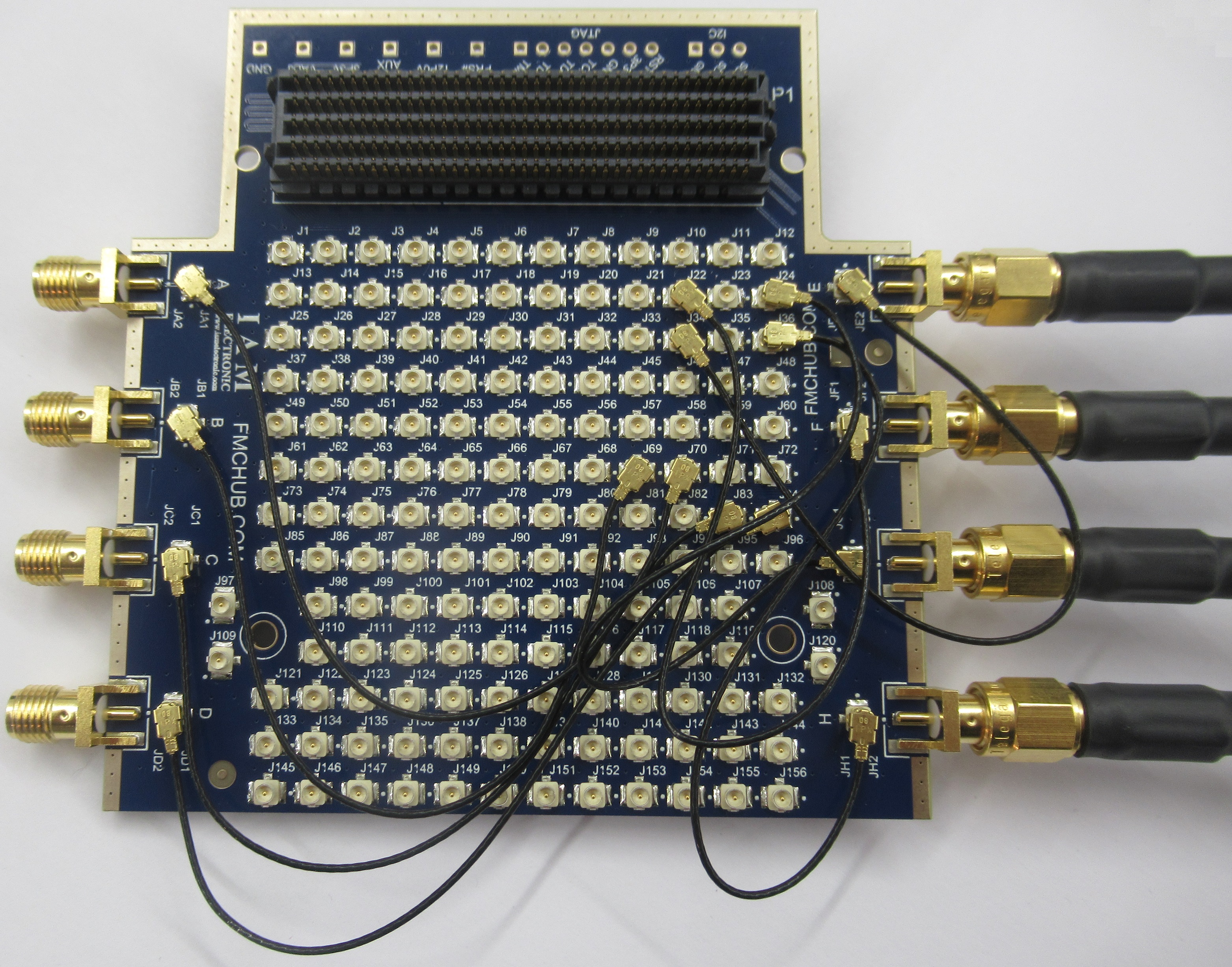 Figure 2.4: High-Speed Probing via U.FL cables and SMA connectors
2.3 Loopback Testing of High-Speed Signals
The FMC debug board supports loopback testing through direct U.FL-to-U.FL cable connections.
This allows developers to test signal paths, validate transceiver behavior, or benchmark link performance under real-world routing conditions.
Advantages:
- Flexible loopback configuration with minimal setup using short U.FL cables
- Datarates up to 6 Gigabit per second
- Enables internal signal routing for diagnostics or bit-error rate (BER) testing
- Efficient for validating signal continuity and protocol integrity
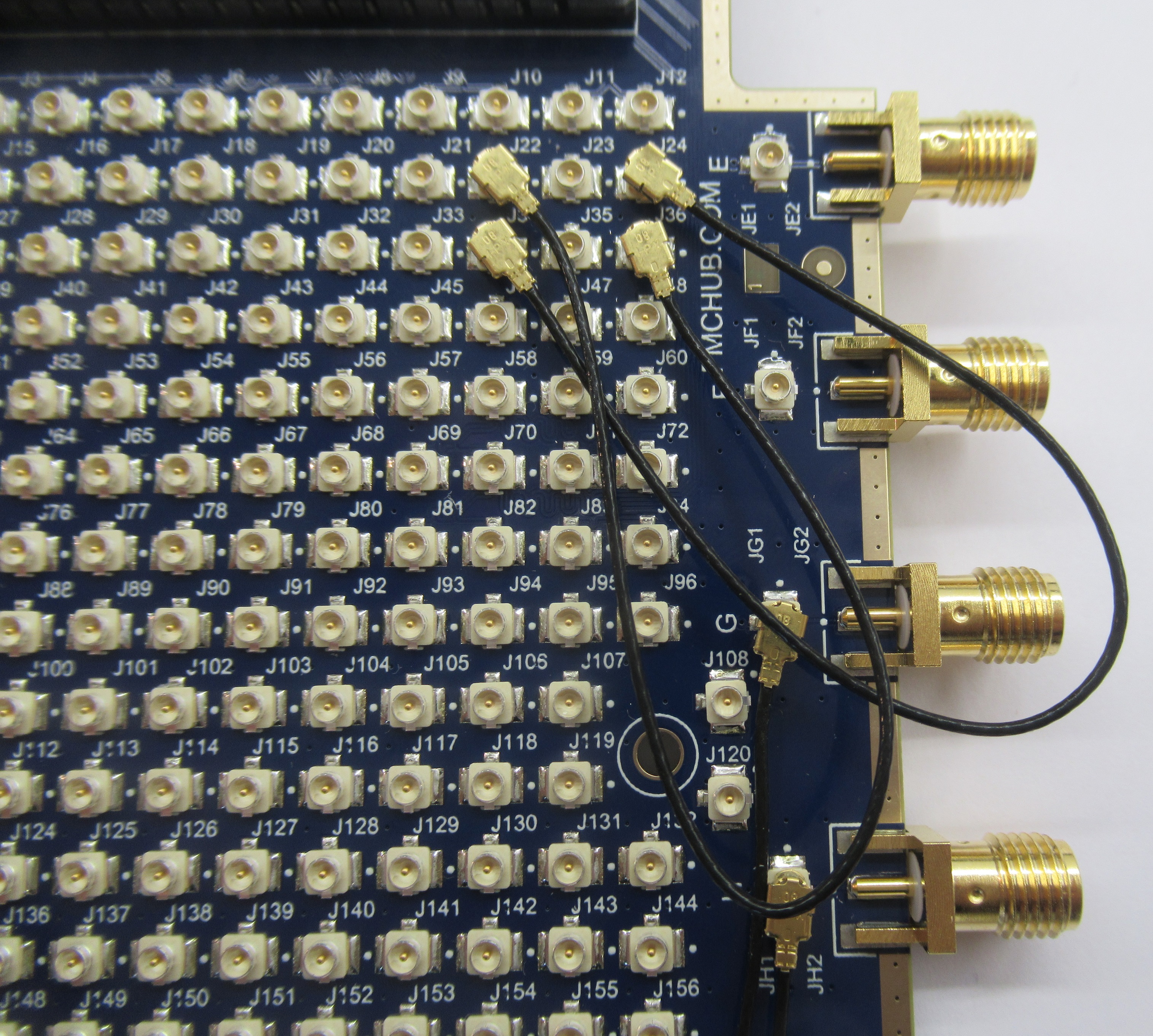 Figure 2.5: Loopback Testing with U.FL Cables
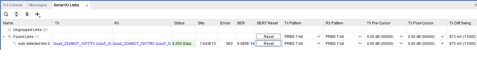 Figure 2.6: U.FL cable loopback. Bit-error rate (BER) testing at 6.25 Gbps
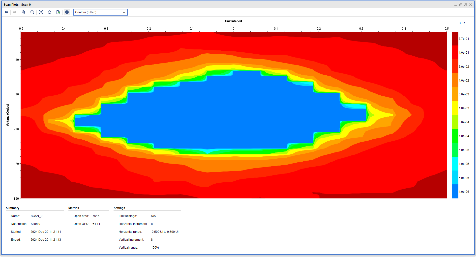 Figure 2.7: U.FL cable loopback. Eye-scan at 6.25 Gbps
2.4 Board-to-Board Connections of FMC Signals The FMC debug board supports board-to-board communication using U.FL cables, SMA cables, or even direct wiring through the clamp connectors. This allows developers to bridge FMC modules, create test setups across multiple FPGAs, or integrate the debug board into a larger multi-board development environment. Advantages:
- Fast reconfiguration of inter-board connections
- Enables distributed system testing or emulation
- Supports differential and single-ended signaling
- Ideal for FPGA-to-FPGA validation or synchronized testing
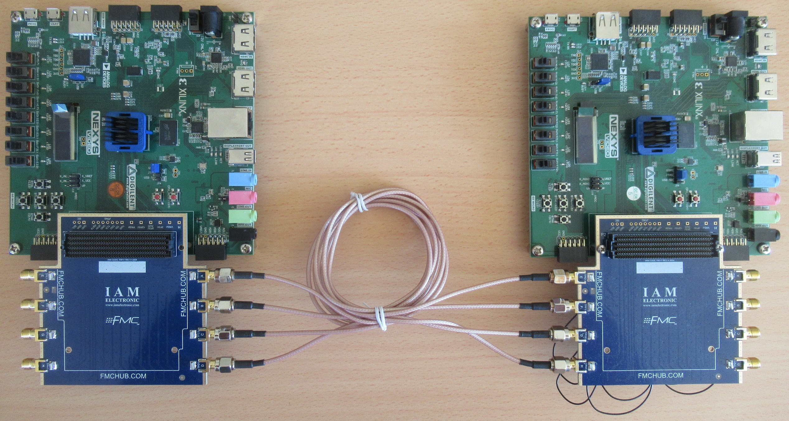 Figure 2.8: Board-to-Board Interconnection Example
2.5 General Information
The board is supplied with 8 U.FL cables to support common probing and interconnection tasks.
Users are responsible for configuring the routing using these cables or compatible jumpers.
It is recommended to connect the U.FL test points of the FMC signals to the SMA/clamp connections using the cables supplied.
To ensure mechanical safety and electrical reliability, spacers or standoffs should be installed when mounting the board to an FMC carrier or chassis.
This prevents connector damage and minimizes mechanical stress.
The scope of delivery includes 8 U.FL cables and a mounting kit with spacers and screws.
Note that the debug board's mechanical dimensions do not comply with the FMC single-width standard.
Due to extended breakout areas and connector placement, users must verify fitment with mechanical enclosures or adjacent components on the carrier board.
The board includes breakout pad arrays for JTAG and I2C access and a dedicated power pin array.
Where needed, users are encouraged to solder standard 2.54 mm pin headers to these locations.
The PCB layout supports common through-hole headers for flexible system integration and extension.
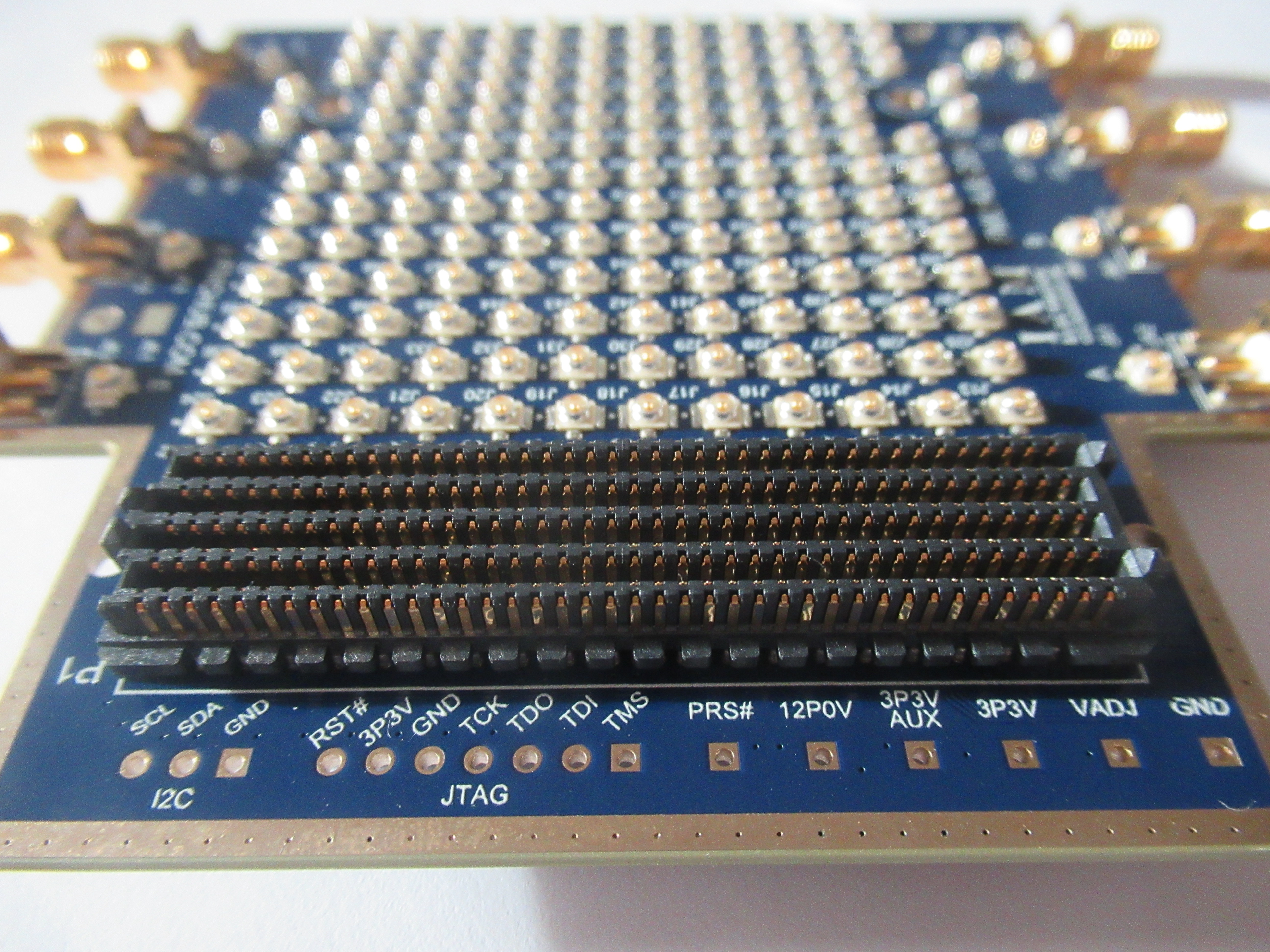 Figure 2.9: Breakout pad arrays for JTAG, I2C, and power pins
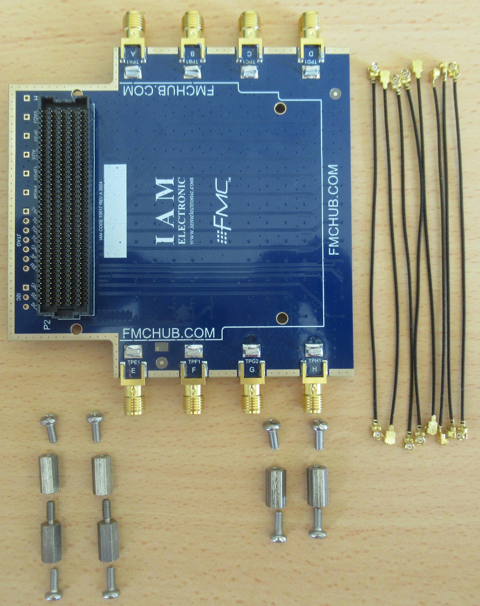 Figure 2.10: FMC HPC-U.FL Debug Board with included accessories. The set includes the circuit board, 8 U.FL cables and a mounting kit with spacers and screws.
This section details the electrical design information, including signal routing characteristics, connector mapping, and reference documentation.
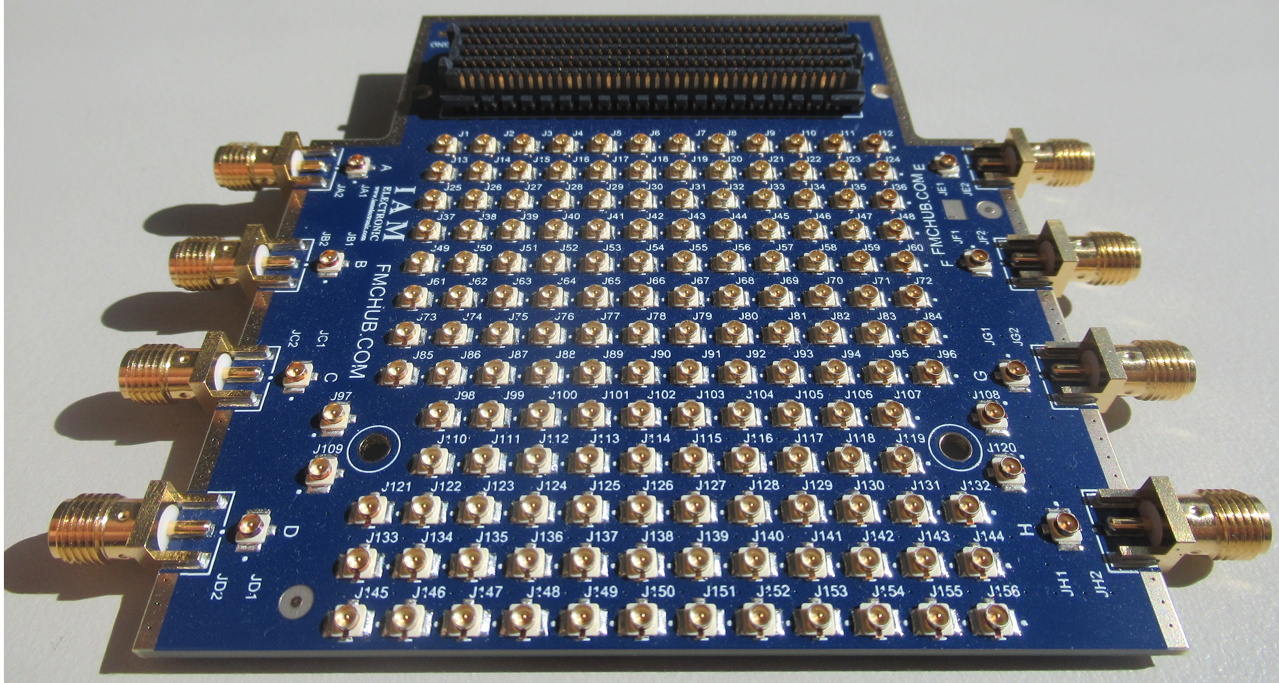
3.1 Signal Mapping to U.FL connectors Table 3.1: U.FL connectors to FMC signals assignment (sorted by connector #id).
| Connector | FMC Pin | FMC Signal Name | Bank | Routed length (mm) | Delay (ps) |
| J1 | A26 | DP2_C2M_P | DP_2 | 94,31 | 520,008 |
| J2 | A27 | DP2_C2M_N | DP_2 | 94,3 | 519,947 |
| J3 | A30 | DP3_C2M_P | DP_3 | 69,843 | 488,574 |
| J4 | A31 | DP3_C2M_N | DP_3 | 69,796 | 488,362 |
| J5 | A34 | DP4_C2M_P | DP_4 | 81,039 | 570,434 |
| J6 | A35 | DP4_C2M_N | DP_4 | 81,038 | 570,36 |
| J7 | B36 | DP6_C2M_P | DP_6 | 97,897 | 540,472 |
| J8 | B37 | DP6_C2M_N | DP_6 | 97,88 | 540,377 |
| J9 | A38 | DP5_C2M_P | DP_5 | 92,455 | 509,424 |
| J10 | A39 | DP5_C2M_N | DP_5 | 92,427 | 509,263 |
| J11 | K23 | HA23_N | HA | 58,702 | 344,537 |
| J12 | K22 | HA23_P | HA | 58,628 | 344,092 |
| J13 | D18 | LA13_N | LA | 72,524 | 503,013 |
| J14 | D26 | LA26_P | LA | 55,929 | 382,769 |
| J15 | D20 | LA17_P_CC | LA | 53,119 | 362,364 |
| J16 | F17 | HA15_N | HA | 48,354 | 327,935 |
| J17 | E16 | HA16_N | HA | 49,328 | 334,831 |
| J18 | F11 | HA08_N | HA | 45,7 | 308,492 |
| J19 | D8 | LA01_P_CC | LA | 112,277 | 791,942 |
| J20 | F5 | HA00_N_CC | HA | 58,205 | 399,819 |
| J21 | E7 | HA05_N | HA | 50,453 | 343,004 |
| J22 | C6 | DP0_M2C_P | DP_0 | 74,716 | 523,992 |
| J23 | D5 | GBTCLK0_M2C_N | GBTCLK_0 | 74,346 | 521,305 |
| J24 | C3 | DP0_C2M_N | DP_0 | 65,647 | 458,08 |
| J25 | D17 | LA13_P | LA | 72,542 | 503,406 |
| J26 | D27 | LA26_N | LA | 55,954 | 382,948 |
| J27 | D21 | LA17_N_CC | LA | 53,212 | 363,041 |
| J28 | F16 | HA15_P | HA | 48,399 | 327,734 |
| J29 | E15 | HA16_P | HA | 49,297 | 334,605 |
| J30 | F10 | HA08_P | HA | 45,622 | 307,92 |
| J31 | D9 | LA01_N_CC | LA | 112,529 | 793,769 |
| J32 | F4 | HA00_P_CC | HA | 58,3 | 399,73 |
| J33 | E6 | HA05_P | HA | 50,476 | 342,918 |
| J34 | C7 | DP0_M2C_N | DP_0 | 74,253 | 520,627 |
| J35 | D4 | GBTCLK0_M2C_P | GBTCLK_0 | 74,417 | 521,82 |
| J36 | C2 | DP0_C2M_P | DP_0 | 65,886 | 459,817 |
| J37 | D15 | LA09_N | LA | 88,386 | 618,455 |
| J38 | C27 | LA27_N | LA | 63,545 | 438,07 |
| J39 | C22 | LA18_P_CC | LA | 55,427 | 379,123 |
| J40 | E18 | HA20_P | HA | 56,402 | 385,95 |
| J41 | F14 | HA12_N | HA | 51,258 | 348,85 |
| J42 | E10 | HA09_N | HA | 57,391 | 393,386 |
| J43 | C10 | LA06_P | LA | 110,664 | 780,224 |
| J44 | E3 | HA01_N_CC | HA | 50,329 | 342,043 |
| J45 | A10 | DP3_M2C_P | DP_3 | 88,901 | 489,14 |
| J46 | A11 | DP3_M2C_N | DP_3 | 88,934 | 489,33 |
| J47 | B16 | DP6_M2C_P | DP_6 | 81,399 | 455,394 |
| J48 | B17 | DP6_M2C_N | DP_6 | 81,375 | 455,255 |
| J49 | D14 | LA09_P | LA | 88,403 | 618,58 |
| J50 | C26 | LA27_P | LA | 63,536 | 438,007 |
| J51 | C23 | LA18_N_CC | LA | 55,48 | 379,51 |
| J52 | E19 | HA20_N | HA | 56,198 | 384,721 |
| J53 | F13 | HA12_P | HA | 51,259 | 348,604 |
| J54 | E9 | HA09_P | HA | 57,371 | 393,24 |
| J55 | C11 | LA06_N | LA | 110,61 | 779,932 |
| J56 | E2 | HA01_P_CC | HA | 50,37 | 342,477 |
| J57 | A14 | DP4_M2C_P | DP_4 | 81,492 | 455,921 |
| J58 | A15 | DP4_M2C_N | DP_4 | 81,754 | 457,416 |
| J59 | A18 | DP5_M2C_P | DP_5 | 81,709 | 457,162 |
| J60 | A19 | DP5_M2C_N | DP_5 | 81,62 | 456,656 |
| J61 | C15 | LA10_N | LA | 100,809 | 708,769 |
| J62 | C19 | LA14_N | LA | 86,443 | 604,345 |
| J63 | D23 | LA23_P | LA | 61,244 | 421,335 |
| J64 | F19 | HA19_P | HA | 60,807 | 418,11 |
| J65 | E13 | HA13_N | HA | 56,931 | 390,043 |
| J66 | F8 | HA04_N | HA | 60,597 | 416,665 |
| J67 | D11 | LA05_P | LA | 110,349 | 777,938 |
| J68 | G3 | CLK1_M2C_N | CLK_1 | 58,715 | 403,135 |
| J69 | A2 | DP1_M2C_P | DP_1 | 92,583 | 519,207 |
| J70 | A3 | DP1_M2C_N | DP_1 | 82,241 | 460,196 |
| J71 | B20 | GBTCLK1_M2C_P | GBTCLK_1 | 89,27 | 491,246 |
| J72 | B21 | GBTCLK1_M2C_N | GBTCLK_1 | 89,282 | 491,314 |
| J73 | C14 | LA10_P | LA | 100,961 | 709,863 |
| J74 | C18 | LA14_P | LA | 86,411 | 604,092 |
| J75 | D24 | LA23_N | LA | 61,28 | 421,624 |
| J76 | F20 | HA19_N | HA | 60,765 | 417,885 |
| J77 | E12 | HA13_P | HA | 57,017 | 390,67 |
| J78 | F7 | HA04_P | HA | 60,708 | 417,358 |
| J79 | D12 | LA05_N | LA | 110,361 | 778,026 |
| J80 | G2 | CLK1_M2C_P | CLK_1 | 58,673 | 403,155 |
| J81 | A6 | DP2_M2C_P | DP_2 | 91,805 | 514,768 |
| J82 | A7 | DP2_M2C_N | DP_2 | 91,721 | 514,287 |
| J83 | A22 | DP1_C2M_P | DP_1 | 92,299 | 517,588 |
| J84 | A23 | DP1_C2M_N | DP_1 | 82,186 | 459,886 |
| J85 | G37 | LA33_N | LA | 60,564 | 421,835 |
| J86 | G34 | LA31_N | LA | 57,384 | 398,599 |
| J87 | G31 | LA29_N | LA | 56,615 | 392,78 |
| J88 | G28 | LA25_N | LA | 56,076 | 389,099 |
| J89 | G25 | LA22_N | LA | 55,601 | 386,102 |
| J90 | G22 | LA20_N | LA | 56,477 | 391,886 |
| J91 | G19 | LA16_N | LA | 56,12 | 389,32 |
| J92 | G15 | LA12_P | LA | 57,061 | 396,602 |
| J93 | G12 | LA08_P | LA | 58,663 | 408,193 |
| J94 | G9 | LA03_P | LA | 60,018 | 418,057 |
| J95 | G6 | LA00_P_CC | LA | 62,433 | 435,365 |
| J96 | H4 | CLK0_M2C_P | CLK_0 | 69,137 | 484,005 |
| J97 | G36 | LA33_P | LA | 60,46 | 420,685 |
| J98 | G33 | LA31_P | LA | 57,126 | 396,872 |
| J99 | G30 | LA29_P | LA | 56,693 | 393,58 |
| J100 | G27 | LA25_P | LA | 56,016 | 389,117 |
| J101 | G24 | LA22_P | LA | 55,668 | 386,236 |
| J102 | G21 | LA20_P | LA | 56,241 | 390,337 |
| J103 | G18 | LA16_P | LA | 56,414 | 391,524 |
| J104 | G16 | LA12_N | LA | 57,079 | 396,568 |
| J105 | G13 | LA08_N | LA | 58,565 | 407,176 |
| J106 | G10 | LA03_N | LA | 60,062 | 418,191 |
| J107 | G7 | LA00_N_CC | LA | 62,486 | 435,641 |
| J108 | H5 | CLK0_M2C_N | CLK_0 | 69,122 | 484,112 |
| J109 | H37 | LA32_P | LA | 72,738 | 509,988 |
| J110 | H34 | LA30_P | LA | 66,931 | 467,955 |
| J111 | H31 | LA28_P | LA | 65,727 | 458,957 |
| J112 | H28 | LA24_P | LA | 65,069 | 454,422 |
| J113 | H25 | LA21_P | LA | 64,976 | 453,849 |
| J114 | H22 | LA19_P | LA | 64,942 | 453,588 |
| J115 | H19 | LA15_P | LA | 65,319 | 456,201 |
| J116 | H16 | LA11_P | LA | 65,623 | 458,335 |
| J117 | H13 | LA07_P | LA | 67,552 | 472,601 |
| J118 | H10 | LA04_P | LA | 69,091 | 483,783 |
| J119 | H7 | LA02_P | LA | 71,544 | 501,367 |
| J120 | J2 | CLK3_M2C_P | CLK_3 | 70,346 | 405,208 |
| J121 | H38 | LA32_N | LA | 72,739 | 510,109 |
| J122 | H35 | LA30_N | LA | 66,944 | 467,629 |
| J123 | H32 | LA28_N | LA | 65,75 | 459,378 |
| J124 | H29 | LA24_N | LA | 65,096 | 454,629 |
| J125 | H26 | LA21_N | LA | 64,916 | 453,143 |
| J126 | H23 | LA19_N | LA | 64,906 | 453,065 |
| J127 | H20 | LA15_N | LA | 65,55 | 457,573 |
| J128 | H17 | LA11_N | LA | 65,935 | 460,469 |
| J129 | H14 | LA07_N | LA | 67,476 | 471,912 |
| J130 | H11 | LA04_N | LA | 69,043 | 483,285 |
| J131 | H8 | LA02_N | LA | 71,623 | 501,692 |
| J132 | J3 | CLK3_M2C_N | CLK_3 | 70,341 | 405,174 |
| J133 | J21 | HA22_P | HA | 84,145 | 488,445 |
| J134 | K19 | HA21_P | HA | 81,885 | 474,816 |
| J135 | J18 | HA18_P | HA | 82,95 | 481,239 |
| J136 | K16 | HA17_P_CC | HA | 79,301 | 459,227 |
| J137 | J15 | HA14_P | HA | 80,12 | 464,167 |
| J138 | K13 | HA10_P | HA | 76,601 | 442,937 |
| J139 | J12 | HA11_P | HA | 77,784 | 450,075 |
| J140 | K10 | HA06_P | HA | 74,074 | 427,697 |
| J141 | J9 | HA07_P | HA | 75,83 | 438,29 |
| J142 | J7 | HA03_N | HA | 75,238 | 434,716 |
| J143 | J6 | HA03_P | HA | 75,099 | 433,881 |
| J144 | K4 | CLK2_M2C_P | CLK_2 | 77,11 | 446,01 |
| J145 | J22 | HA22_N | HA | 84,282 | 489,277 |
| J146 | K20 | HA21_N | HA | 81,811 | 474,371 |
| J147 | J19 | HA18_N | HA | 82,917 | 481,041 |
| J148 | K17 | HA17_N_CC | HA | 79,299 | 459,217 |
| J149 | J16 | HA14_N | HA | 80,159 | 464,405 |
| J150 | K14 | HA10_N | HA | 76,755 | 443,871 |
| J151 | J13 | HA11_N | HA | 77,713 | 449,648 |
| J152 | K11 | HA06_N | HA | 74,19 | 428,395 |
| J153 | J10 | HA07_N | HA | 75,843 | 438,367 |
| J154 | K8 | HA02_N | HA | 78,29 | 453,13 |
| J155 | K7 | HA02_P | HA | 78,313 | 453,265 |
| J156 | K5 | CLK2_M2C_N | CLK_2 | 77,122 | 446,083 |
| FMC Signal Name | FMC Pin | Connector | Bank | Routed length (mm) | Delay (ps) |
| CLK0_M2C_N | H5 | J108 | CLK_0 | 69,122 | 484,112 |
| CLK0_M2C_P | H4 | J96 | CLK_0 | 69,137 | 484,005 |
| CLK1_M2C_N | G3 | J68 | CLK_1 | 58,715 | 403,135 |
| CLK1_M2C_P | G2 | J80 | CLK_1 | 58,673 | 403,155 |
| CLK2_M2C_N | K5 | J156 | CLK_2 | 77,122 | 446,083 |
| CLK2_M2C_P | K4 | J144 | CLK_2 | 77,11 | 446,01 |
| CLK3_M2C_N | J3 | J132 | CLK_3 | 70,341 | 405,174 |
| CLK3_M2C_P | J2 | J120 | CLK_3 | 70,346 | 405,208 |
| DP0_C2M_N | C3 | J24 | DP_0 | 65,647 | 458,08 |
| DP0_C2M_P | C2 | J36 | DP_0 | 65,886 | 459,817 |
| DP0_M2C_N | C7 | J34 | DP_0 | 74,253 | 520,627 |
| DP0_M2C_P | C6 | J22 | DP_0 | 74,716 | 523,992 |
| DP1_C2M_N | A23 | J84 | DP_1 | 82,186 | 459,886 |
| DP1_C2M_P | A22 | J83 | DP_1 | 92,299 | 517,588 |
| DP1_M2C_N | A3 | J70 | DP_1 | 82,241 | 460,196 |
| DP1_M2C_P | A2 | J69 | DP_1 | 92,583 | 519,207 |
| DP2_C2M_N | A27 | J2 | DP_2 | 94,3 | 519,947 |
| DP2_C2M_P | A26 | J1 | DP_2 | 94,31 | 520,008 |
| DP2_M2C_N | A7 | J82 | DP_2 | 91,721 | 514,287 |
| DP2_M2C_P | A6 | J81 | DP_2 | 91,805 | 514,768 |
| DP3_C2M_N | A31 | J4 | DP_3 | 69,796 | 488,362 |
| DP3_C2M_P | A30 | J3 | DP_3 | 69,843 | 488,574 |
| DP3_M2C_N | A11 | J46 | DP_3 | 88,934 | 489,33 |
| DP3_M2C_P | A10 | J45 | DP_3 | 88,901 | 489,14 |
| DP4_C2M_N | A35 | J6 | DP_4 | 81,038 | 570,36 |
| DP4_C2M_P | A34 | J5 | DP_4 | 81,039 | 570,434 |
| DP4_M2C_N | A15 | J58 | DP_4 | 81,754 | 457,416 |
| DP4_M2C_P | A14 | J57 | DP_4 | 81,492 | 455,921 |
| DP5_C2M_N | A39 | J10 | DP_5 | 92,427 | 509,263 |
| DP5_C2M_P | A38 | J9 | DP_5 | 92,455 | 509,424 |
| DP5_M2C_N | A19 | J60 | DP_5 | 81,62 | 456,656 |
| DP5_M2C_P | A18 | J59 | DP_5 | 81,709 | 457,162 |
| DP6_C2M_N | B37 | J8 | DP_6 | 97,88 | 540,377 |
| DP6_C2M_P | B36 | J7 | DP_6 | 97,897 | 540,472 |
| DP6_M2C_N | B17 | J48 | DP_6 | 81,375 | 455,255 |
| DP6_M2C_P | B16 | J47 | DP_6 | 81,399 | 455,394 |
| GBTCLK0_M2C_N | D5 | J23 | GBTCLK_0 | 74,346 | 521,305 |
| GBTCLK0_M2C_P | D4 | J35 | GBTCLK_0 | 74,417 | 521,82 |
| GBTCLK1_M2C_N | B21 | J72 | GBTCLK_1 | 89,282 | 491,314 |
| GBTCLK1_M2C_P | B20 | J71 | GBTCLK_1 | 89,27 | 491,246 |
| HA00_N_CC | F5 | J20 | HA | 58,205 | 399,819 |
| HA00_P_CC | F4 | J32 | HA | 58,3 | 399,73 |
| HA01_N_CC | E3 | J44 | HA | 50,329 | 342,043 |
| HA01_P_CC | E2 | J56 | HA | 50,37 | 342,477 |
| HA02_N | K8 | J154 | HA | 78,29 | 453,13 |
| HA02_P | K7 | J155 | HA | 78,313 | 453,265 |
| HA03_N | J7 | J142 | HA | 75,238 | 434,716 |
| HA03_P | J6 | J143 | HA | 75,099 | 433,881 |
| HA04_N | F8 | J66 | HA | 60,597 | 416,665 |
| HA04_P | F7 | J78 | HA | 60,708 | 417,358 |
| HA05_N | E7 | J21 | HA | 50,453 | 343,004 |
| HA05_P | E6 | J33 | HA | 50,476 | 342,918 |
| HA06_N | K11 | J152 | HA | 74,19 | 428,395 |
| HA06_P | K10 | J140 | HA | 74,074 | 427,697 |
| HA07_N | J10 | J153 | HA | 75,843 | 438,367 |
| HA07_P | J9 | J141 | HA | 75,83 | 438,29 |
| HA08_N | F11 | J18 | HA | 45,7 | 308,492 |
| HA08_P | F10 | J30 | HA | 45,622 | 307,92 |
| HA09_N | E10 | J42 | HA | 57,391 | 393,386 |
| HA09_P | E9 | J54 | HA | 57,371 | 393,24 |
| HA10_N | K14 | J150 | HA | 76,755 | 443,871 |
| HA10_P | K13 | J138 | HA | 76,601 | 442,937 |
| HA11_N | J13 | J151 | HA | 77,713 | 449,648 |
| HA11_P | J12 | J139 | HA | 77,784 | 450,075 |
| HA12_N | F14 | J41 | HA | 51,258 | 348,85 |
| HA12_P | F13 | J53 | HA | 51,259 | 348,604 |
| HA13_N | E13 | J65 | HA | 56,931 | 390,043 |
| HA13_P | E12 | J77 | HA | 57,017 | 390,67 |
| HA14_N | J16 | J149 | HA | 80,159 | 464,405 |
| HA14_P | J15 | J137 | HA | 80,12 | 464,167 |
| HA15_N | F17 | J16 | HA | 48,354 | 327,935 |
| HA15_P | F16 | J28 | HA | 48,399 | 327,734 |
| HA16_N | E16 | J17 | HA | 49,328 | 334,831 |
| HA16_P | E15 | J29 | HA | 49,297 | 334,605 |
| HA17_N_CC | K17 | J148 | HA | 79,299 | 459,217 |
| HA17_P_CC | K16 | J136 | HA | 79,301 | 459,227 |
| HA18_N | J19 | J147 | HA | 82,917 | 481,041 |
| HA18_P | J18 | J135 | HA | 82,95 | 481,239 |
| HA19_N | F20 | J76 | HA | 60,765 | 417,885 |
| HA19_P | F19 | J64 | HA | 60,807 | 418,11 |
| HA20_N | E19 | J52 | HA | 56,198 | 384,721 |
| HA20_P | E18 | J40 | HA | 56,402 | 385,95 |
| HA21_N | K20 | J146 | HA | 81,811 | 474,371 |
| HA21_P | K19 | J134 | HA | 81,885 | 474,816 |
| HA22_N | J22 | J145 | HA | 84,282 | 489,277 |
| HA22_P | J21 | J133 | HA | 84,145 | 488,445 |
| HA23_N | K23 | J11 | HA | 58,702 | 344,537 |
| HA23_P | K22 | J12 | HA | 58,628 | 344,092 |
| LA00_N_CC | G7 | J107 | LA | 62,486 | 435,641 |
| LA00_P_CC | G6 | J95 | LA | 62,433 | 435,365 |
| LA01_N_CC | D9 | J31 | LA | 112,529 | 793,769 |
| LA01_P_CC | D8 | J19 | LA | 112,277 | 791,942 |
| LA02_N | H8 | J131 | LA | 71,623 | 501,692 |
| LA02_P | H7 | J119 | LA | 71,544 | 501,367 |
| LA03_N | G10 | J106 | LA | 60,062 | 418,191 |
| LA03_P | G9 | J94 | LA | 60,018 | 418,057 |
| LA04_N | H11 | J130 | LA | 69,043 | 483,285 |
| LA04_P | H10 | J118 | LA | 69,091 | 483,783 |
| LA05_N | D12 | J79 | LA | 110,361 | 778,026 |
| LA05_P | D11 | J67 | LA | 110,349 | 777,938 |
| LA06_N | C11 | J55 | LA | 110,61 | 779,932 |
| LA06_P | C10 | J43 | LA | 110,664 | 780,224 |
| LA07_N | H14 | J129 | LA | 67,476 | 471,912 |
| LA07_P | H13 | J117 | LA | 67,552 | 472,601 |
| LA08_N | G13 | J105 | LA | 58,565 | 407,176 |
| LA08_P | G12 | J93 | LA | 58,663 | 408,193 |
| LA09_N | D15 | J37 | LA | 88,386 | 618,455 |
| LA09_P | D14 | J49 | LA | 88,403 | 618,58 |
| LA10_N | C15 | J61 | LA | 100,809 | 708,769 |
| LA10_P | C14 | J73 | LA | 100,961 | 709,863 |
| LA11_N | H17 | J128 | LA | 65,935 | 460,469 |
| LA11_P | H16 | J116 | LA | 65,623 | 458,335 |
| LA12_N | G16 | J104 | LA | 57,079 | 396,568 |
| LA12_P | G15 | J92 | LA | 57,061 | 396,602 |
| LA13_N | D18 | J13 | LA | 72,524 | 503,013 |
| LA13_P | D17 | J25 | LA | 72,542 | 503,406 |
| LA14_N | C19 | J62 | LA | 86,443 | 604,345 |
| LA14_P | C18 | J74 | LA | 86,411 | 604,092 |
| LA15_N | H20 | J127 | LA | 65,55 | 457,573 |
| LA15_P | H19 | J115 | LA | 65,319 | 456,201 |
| LA16_N | G19 | J91 | LA | 56,12 | 389,32 |
| LA16_P | G18 | J103 | LA | 56,414 | 391,524 |
| LA17_N_CC | D21 | J27 | LA | 53,212 | 363,041 |
| LA17_P_CC | D20 | J15 | LA | 53,119 | 362,364 |
| LA18_N_CC | C23 | J51 | LA | 55,48 | 379,51 |
| LA18_P_CC | C22 | J39 | LA | 55,427 | 379,123 |
| LA19_N | H23 | J126 | LA | 64,906 | 453,065 |
| LA19_P | H22 | J114 | LA | 64,942 | 453,588 |
| LA20_N | G22 | J90 | LA | 56,477 | 391,886 |
| LA20_P | G21 | J102 | LA | 56,241 | 390,337 |
| LA21_N | H26 | J125 | LA | 64,916 | 453,143 |
| LA21_P | H25 | J113 | LA | 64,976 | 453,849 |
| LA22_N | G25 | J89 | LA | 55,601 | 386,102 |
| LA22_P | G24 | J101 | LA | 55,668 | 386,236 |
| LA23_N | D24 | J75 | LA | 61,28 | 421,624 |
| LA23_P | D23 | J63 | LA | 61,244 | 421,335 |
| LA24_N | H29 | J124 | LA | 65,096 | 454,629 |
| LA24_P | H28 | J112 | LA | 65,069 | 454,422 |
| LA25_N | G28 | J88 | LA | 56,076 | 389,099 |
| LA25_P | G27 | J100 | LA | 56,016 | 389,117 |
| LA26_N | D27 | J26 | LA | 55,954 | 382,948 |
| LA26_P | D26 | J14 | LA | 55,929 | 382,769 |
| LA27_N | C27 | J38 | LA | 63,545 | 438,07 |
| LA27_P | C26 | J50 | LA | 63,536 | 438,007 |
| LA28_N | H32 | J123 | LA | 65,75 | 459,378 |
| LA28_P | H31 | J111 | LA | 65,727 | 458,957 |
| LA29_N | G31 | J87 | LA | 56,615 | 392,78 |
| LA29_P | G30 | J99 | LA | 56,693 | 393,58 |
| LA30_N | H35 | J122 | LA | 66,944 | 467,629 |
| LA30_P | H34 | J110 | LA | 66,931 | 467,955 |
| LA31_N | G34 | J86 | LA | 57,384 | 398,599 |
| LA31_P | G33 | J98 | LA | 57,126 | 396,872 |
| LA32_N | H38 | J121 | LA | 72,739 | 510,109 |
| LA32_P | H37 | J109 | LA | 72,738 | 509,988 |
| LA33_N | G37 | J85 | LA | 60,564 | 421,835 |
| LA33_P | G36 | J97 | LA | 60,46 | 420,685 |
3.2 Reference Files To ensure reproducibility and allow community collaboration, all hardware design files are made publicly available: Schematics: T0017_HPC_UFL_DEBUG_BOARD_SCHEMATICS_2024_12_13_REV_A.pdf PCB Layers: T0017_HPC_UFL_DEBUG_BOARD_LAYERS_2024_12_13_REV_A.pdf Mechanical drawings: T0017_HPC_UFL_DEBUG_BOARD_MECHANICAL_2024_12_13_REV_A.pdf GitHub Repository: https://github.com/FMCHUB/FMC_HPC_UFL_DEBUG_BOARD
3.3 Bill of Materials (BoM) Table 3.3: Parts List
| Item No. | Component Description | Manufacturer | Part Number | Quantity |
| 1 | CC-HPC-10 | Samtec | ASP-134486-01 | 1 |
| 2 | MC-HPC-10 | Samtec | ASP-134488-01 | 1 |
| 3 | RF Coax Connector, U.FL Jack | Hirose Electric | U-FL-R-SMT-1 | 164 |
| 4 | SMA Edge Mount | Samtec | SMA-J-P-H-ST-EM1 | 8 |
| 5 | Clamp Testpoints | Keystone Electronic | 5095 | 8 |
| 6 | U.FL RF Cable Assembly, Length .1 m | TE Connectivity | 2015699-1 | 8 |
| 7 | Screwed spacer, 10mm, Int.thread: M2.5, hexagonal | Dremec | 142X10 | 4 |
| 8 | Screwed spacer, 10mm, Int.thread: M2.5, Ext.thread: M2.5 | Dremec | 242X10 | 2 |
| 9 | Screw M2.5 x 6mm, stainless steel, length: 6mm, head diameter: 5mm | Standard | Standard | 8 |
The board outline exceed the size defined by ANSI/VITA 57.1 standard for single width FMC modules. A single width FMC module with board dimensions of 78.80 mm x 69 mm can be attached on top of the debug board.
Exact dimensions are given in figure 4.1
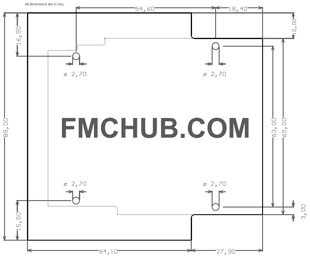 Fig. 4.1: Mechanical drawing of the FMC HPC-U.FL Debug Board.
The mounting holes are plated. Their sizes and positions are in accordance with ANSI/VITA 57.1 single width FMC modules with commercial grade mounting (air cooled).
Fig. 4.1: Mechanical drawing of the FMC HPC-U.FL Debug Board.
The mounting holes are plated. Their sizes and positions are in accordance with ANSI/VITA 57.1 single width FMC modules with commercial grade mounting (air cooled).
| Product no. | Description | Market place | Request quote | Standard lead time |
| T0017 | FMC HPC-U.FL Debug Board with both MC-HPC-10 and CC-HPC-10 connectors on bottom and top side. | IAM Electronic Shop Ebay #187227314198 Tindie#38762 DigiKey6068-T0017-ND | info@iamelectronic.com | Normally in stock, 6 weeks |